Array antenna structure and multilayer via-hole structure

An array antenna and via technology, which is applied in the electronic field, can solve the problems of high profile, uncompact structure, and narrow bandwidth, and achieve the effect of improving reflection parameters, increasing bandwidth, and solving efficient interconnection

Active Publication Date: 2018-01-09
SOUTHEAST UNIV
View PDF8 Cites 32 Cited by
  • Summary
  • Abstract
  • Description
  • Claims
  • Application Information

AI Technical Summary

Problems solved by technology

[0008] Therefore, the current array antennas with related structures still have problems such as uncompact structure, high profile, narrow bandwidth, etc., and the RF front-end is connected to the antenna in the millimeter-wave RF system using a multi-layer printed circuit board.

Method used


Image

  • Array antenna structure and multilayer via-hole structure
  • Array antenna structure and multilayer via-hole structure
  • Array antenna structure and multilayer via-hole structure

Examples


Embodiment Construction

[0032] The technical solutions and beneficial effects of the present invention will be described in detail below in conjunction with the accompanying drawings.

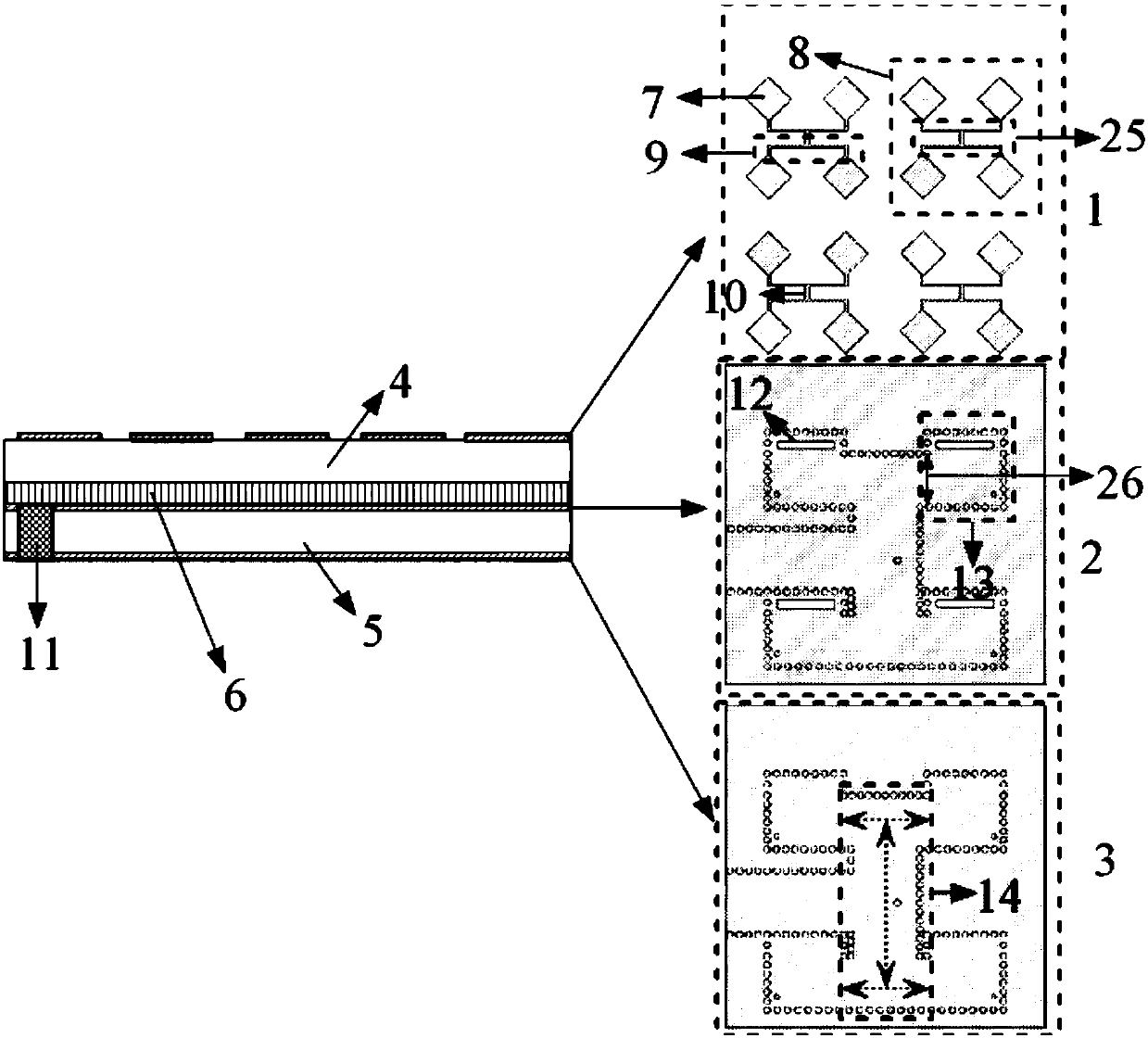
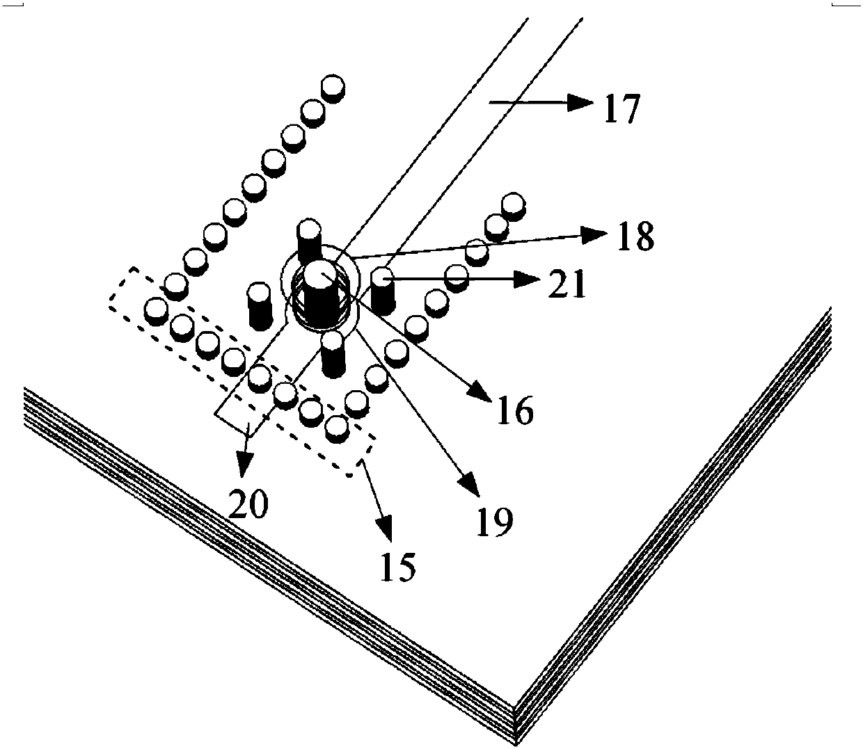
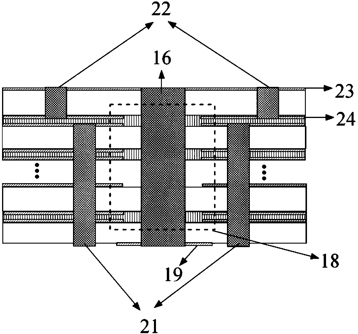
[0033] Such as figure 1As shown, the present invention provides an array antenna structure, including two parts of the radiation unit 1 and the feed network 2, 3, wherein the radiation unit adopts the form of a planar patch, and the feed network adopts the form of a substrate integrated waveguide; the overall structure It is realized by multi-layer printed circuit board technology, and the radiation unit and the feed network are not realized on the same layer of dielectric substrate. In the hierarchical structure of multi-layer printed circuit board, there are two dielectric substrates, three metal layers and one Paste the dielectric layer, from top to bottom are the top metal layer 1, the first dielectric substrate 4, the pasted dielectric layer 6, the middle metal layer 2, the second dielectric substrate 5, and the ...


PUM


Abstract

The invention discloses an array antenna structure, which comprises a radiation unit and a feed network. The radiation unit adopts a plane patch form; the feed network adopts a substrate integrated waveguide form; the overall structure is realized through multilayer printed circuit board technology; and the feed network is characterized by providing a transverse seam in the broad side of the bentsubstrate integrated waveguide, and carrying out feeding on a top metal patch through seam coupling. The invention also discloses a multilayer via-hole structure, which is characterized by closing oneport of the substrate integrated waveguide on some layer of dielectric substrate, and using one plated through hole to transmit radio-frequency signals. Such array antenna structure adopts the bent substrate integrated waveguide transverse seam structure, increases the bandwidth of the array antenna under the condition of realizing a thin dielectric substrate through matching design of the feed network, and realizes that a millimeter wave antenna and a radio frequency front end are on different layers of a multilayer printed circuit board to meet design of a millimeter-wave system having higher requirements for size and width.

Description

technical field [0001] The invention belongs to the field of electronics, and in particular relates to an array antenna structure and a multilayer through-hole transfer structure. Background technique [0002] With the progress of society and the development of technology, the demand for high performance and miniaturization of electronic systems is becoming increasingly urgent. Array antennas are widely used in electronic systems in many fields such as communication, navigation, radar, and detection, and can achieve high performance. The miniaturized array antenna structure will inevitably bring good economic and social benefits. [0003] The microstrip patch antenna is a planar array antenna structure that has developed rapidly in recent decades. It is widely used in various radio application scenarios due to its compact structure, light weight, low cost, and easy integration. When forming an array with a patch antenna, especially when the array is formed to a certain scal...

Claims


Application Information

Patent Timeline
Patent Type & Authority Applications(China)
IPC IPC(8): H01Q21/00H01Q1/38H01Q1/50
Inventor 洪伟徐俊陈继新蒋之浩张慧
Owner SOUTHEAST UNIV
Why Eureka
Try Eureka