MOSFET protection circuit

A technology for protecting circuits and circuits, applied in electrical components, electronic switches, pulse technology, etc., can solve problems such as large parasitic induced voltage, MOSFET overvoltage damage, etc., to reduce reverse induced voltage, delay switching speed, and reduce overvoltage The effect of the risk of harm

Pending Publication Date: 2018-01-09
YUNNAN POWER GRID CO LTD ELECTRIC POWER RES INST
View PDF0 Cites 0 Cited by
  • Summary
  • Abstract
  • Description
  • Claims
  • Application Information

AI Technical Summary

Problems solved by technology

[0005] This application provides a MOSFET protection circuit, which is used to solve the problem that when the MOSFET Q3 is quickly turned off, the ...

Method used


Image

  • MOSFET protection circuit
  • MOSFET protection circuit
  • MOSFET protection circuit

Examples


Embodiment Construction

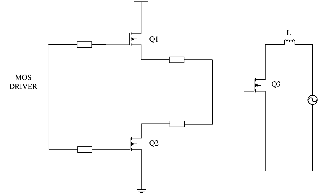
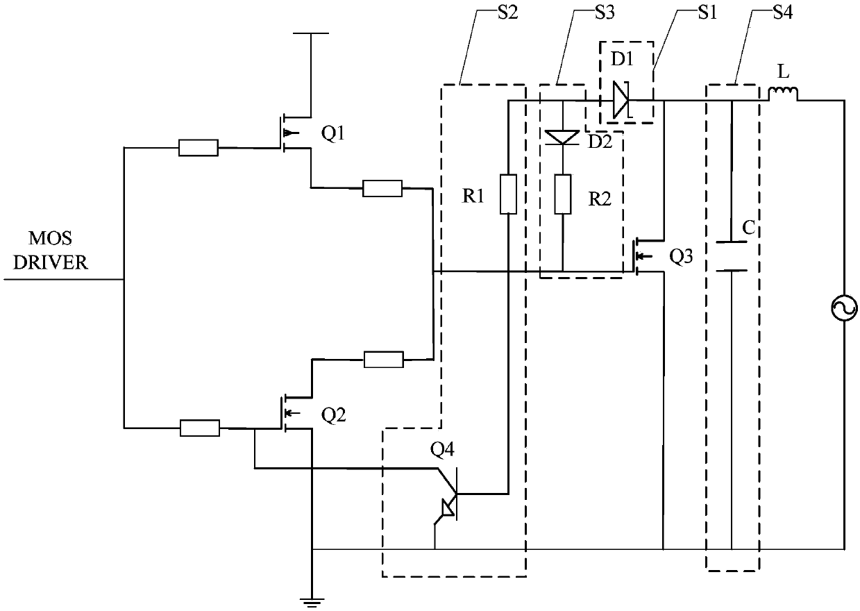
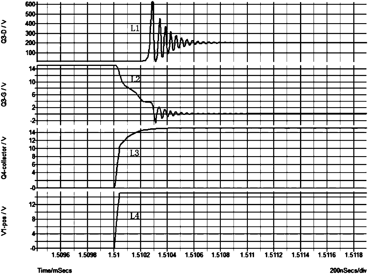
[0025] Such as figure 1 In the switching amplifier shown, MOSFET Q1 and MOSFET Q2 form a push-pull switch, which is used to control MOSFET Q3 to be turned on or off. In order to pursue the performance of the switching amplifier, in current switching amplifiers, the MOSFET Q3 mostly uses a high-power device, and the high-power MOSFET Q3 has a high switching frequency, which can be turned on or off quickly. However, when the high-power MOSFET Q3 is working, the parasitic inductance L existing in the circuit will generate an obvious reverse induced voltage when the MOSFET Q3 switches rapidly, especially when the switching amplifier is over-current or short-circuited, the parasitic inductance L will generate The reverse induced voltage will be higher. The reverse induced voltage and the power supply voltage act together on MOSFET Q3. Once the voltage carried by MOSFET Q1 exceeds the maximum withstand voltage of MOSFET Q1, it will cause overvoltage damage to MOSFET Q3. The presen...


PUM


Abstract

The present application discloses a protection circuit for MOSFET, including a voltage stabilizing circuit S1, a delay circuit S2 and an energy supplementary circuit S3, wherein the voltage stabilizing circuit S1 includes a voltage stabilizing diode D1. The negative pole of the Zener diode D1 is connected to the D pole of the MOSFET Q3, and the positive pole of the Zener diode D1 is respectively connected to the delay circuit S2 and the power supply circuit S3; the other end of the delay circuit S2 is connected to the G pole of the MOSFET Q2, and the other end of the power supply circuit S3 Connect to the G terminal of MOSFET Q3. The protection circuit of the present application reduces the reverse induced voltage generated by the parasitic inductance L by slowing down the switching speed of the MOSFET Q3, thereby reducing the risk of overvoltage of the MOSFET Q3.

Description

technical field [0001] The present application relates to the field of MOSFET protection, in particular to a protection circuit for MOSFET. Background technique [0002] MOSFET (Metal-Oxide-Semiconductor Field-Effect Transistor, Metal-Oxide Semiconductor Field-Effect Transistor) is a field-effect transistor that has been widely used as a current amplifier or switch controller. For example, an amplifier is a device realized by utilizing the ability of a MOSFET to amplify current. [0003] figure 1 is a circuit diagram of a switching amplifier, such as figure 1 As shown, the switching amplifier contains a plurality of MOSFETs, wherein MOSFET Q3 is used to amplify current; MOSFET Q1 and MOSFET Q2 form a push-pull switch, which is used to control MOSFET Q3 to be turned on or off. The use process of the switching amplifier includes: when the driving signal MOS Driver is low voltage, MOSFET Q1 is turned on, so that MOSFET Q3 is turned on; when the driving signal MOS Driver is h...

Claims


Application Information

Patent Timeline
IPC IPC(8): H03K17/08
Inventor 许守东陈勇张丽
Owner YUNNAN POWER GRID CO LTD ELECTRIC POWER RES INST
Why Eureka
Try Eureka