Organic electroluminescent display panel and display device

An electroluminescence display and display panel technology, applied in circuits, electrical components, electric solid-state devices, etc., can solve problems such as voltage increase, achieve low power consumption, long-term stable driving voltage, and long service life

Active Publication Date: 2018-01-12
WUHAN TIANMA MICRO ELECTRONICS CO LTD
View PDF2 Cites 10 Cited by
  • Summary
  • Abstract
  • Description
  • Claims
  • Application Information

AI Technical Summary

Problems solved by technology

[0004] The invention discloses an organic electroluminescent display panel and a display device, which are used to solve the problem th

Method used


Image

  • Organic electroluminescent display panel and display device
  • Organic electroluminescent display panel and display device
  • Organic electroluminescent display panel and display device

Examples


Embodiment 1

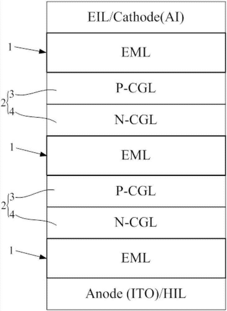
[0057] Embodiment one, such as image 3 As shown, the P-I-N type OLED provided by the embodiment of the present invention may include a first light-emitting unit 11, a second light-emitting unit 12 and a third light-emitting unit 13 connected in series in sequence. The first light-emitting unit 11, the second light-emitting unit 12 and the third light-emitting unit The three light-emitting units 13 can form white light through brightness ratio; optionally, the first light-emitting unit 11, the second light-emitting unit 12 and the third light-emitting unit 13 can be green light-emitting units, red light-emitting units and blue light-emitting units respectively Specifically, a first charge generation layer (P-I-N type CGL) 21 is provided between the first light emitting unit 11 and the second light emitting unit 12, and a second charge generation layer is provided between the second light emitting unit 12 and the third light emitting unit 13 layer (P-I-N type CGL) 22 .

Embodiment approach

[0059] Mode 1, in the first charge generation layer 21, the electron mobility of the intermediate layer (I layer) 51 is greater than the electron mobility of the N-doped layer host material; in the second charge generation layer 22, the electron mobility of the intermediate layer (I layer) 52 The hole mobility is greater than that of the host material of the P-doped layer.

[0060] Mode 2, in the first charge generation layer 21, the hole mobility of the intermediate layer (I layer) 51 is greater than the hole mobility of the P-doped layer host material; in the second charge generation layer 22, the intermediate layer (I layer) The electron mobility of 52 is greater than that of the host material of the N-doped layer.

[0061] Mode 3, in the first charge generation layer 21, the electron mobility of the intermediate layer (I layer) 51 is greater than the electron mobility of the N-doped layer host material; in the second charge generation layer 22, the electron mobility of the...

Embodiment 2

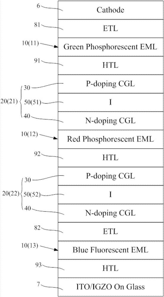
[0063] Embodiment two, such as Figure 4 As shown, the P-I-N type CGL OLED panel provided by the embodiment of the present invention may include two light-emitting units 10 connected in series, that is, the light-emitting unit 14 and the light-emitting unit 15. The light-emitting unit 14 and the light-emitting unit 15 can form white light through brightness ratio Optionally, the light-emitting unit 14 and the light-emitting unit 15 can be respectively a yellow light-emitting unit and a blue light-emitting unit; specifically, a charge generation layer (P-I-N type CGL) 23 is provided between the light-emitting unit 14 and the light-emitting unit 15, the In the charge generation layer (P-I-N type CGL) 23, the electron mobility of the intermediate layer (I layer) 53 is greater than the electron mobility of the host material of the N-doped layer 40; and / or, the hole mobility of the intermediate layer (I layer) 53 The rate is greater than the hole mobility of the host material of th...


PUM

PropertyMeasurementUnit
Electron mobilityaaaaaaaaaa
Mobilityaaaaaaaaaa

Abstract

The invention relates to the field of display technologies, and discloses an organic electroluminescent display panel. The organic electroluminescent display panel comprises a cathode layer, an anodelayer, and at least two light-emitting units which are arranged between the cathode layer and the anode layer and connected in series with each other, wherein a charge generation layer is arranged between the at least one pair of adjacent light-emitting units; the charge generation layer comprises a P-doped layer close to one side of the cathode layer, an N-doped layer close to one side of the anode layer, and an intermediate layer arranged between the P-doped layer and the N-doped layer; and electron mobility of the intermediate layer is greater than electron mobility of host materials of theN-doped layer, and/or, hole mobility of the intermediate is greater than hole mobility of host materials of the P-doped layer. The organic electroluminescent display panel provided by the invention has the advantages of long-term stable driving voltage, low power consumption, long service life and high luminous efficiency.

Description

technical field [0001] The invention relates to the field of display technology, in particular to an organic electroluminescent display panel and a display device. Background technique [0002] Existing white light organic electroluminescent display devices (OLEDs) are mainly based on red-green-blue (R-G-B) three-color or blue-yellow (B-Y) two-color light-emitting units by adjusting the ratio of light-emitting brightness to form white light. At present, white light OLEDs usually adopt a series stacked structure, for example, a red light-emitting unit, a green light-emitting unit and a blue light-emitting unit are connected in series; and, in order to improve the efficiency of OLED devices, charge is generally added between different light-emitting layers Generation layer (CGL, Chargegeneration layer). [0003] Usually, the CGL layer includes a direct contact N-doping layer (N-doping CGL) and P-doping layer (P-doping CGL) two-layer structure, that is, P-N type CGL, however, ...

Claims


Application Information

Patent Timeline
IPC IPC(8): H01L51/50H01L27/32
CPCY04S30/12Y02T90/167
Inventor 马洪虎牛晶华王湘成杨闰
Owner WUHAN TIANMA MICRO ELECTRONICS CO LTD
Why Eureka
Try Eureka