
Pixel structure and liquid crystal display panel

A pixel structure and pixel electrode technology, applied in static indicators, instruments, nonlinear optics, etc., can solve the problems of liquid crystal pre-deflection confusion, increased parasitic capacitance, and poor display effect, achieving good display effect and increased capacity Effect

Active Publication Date: 2018-01-19
SHENZHEN CHINA STAR OPTOELECTRONICS SEMICON DISPLAY TECH CO LTD
View PDF3 Cites 11 Cited by
  • Summary
  • Abstract
  • Description
  • Claims
  • Application Information

AI Technical Summary

Problems solved by technology

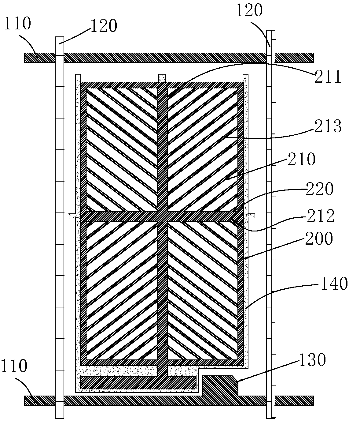
However, due to the expansion of the pixel electrode to the scanning line and the data line, the parasitic capacitance between the pixel electrode, the scanning line and the data line increases, thereby causing the display effect to deteriorate; moreover, since the pixel electrode expands to the scanning line and the data line , make the pixel electrode closer to the black matrix on the color filter substrate (there is a common electrode on the black matrix), so that the liquid crystal between the pixel electrode and the color filter substrate is affected by the topography of the branch electrodes and the topography (slope) of the black matrix Affected, causing liquid crystal pre-deflection confusion, easy to form dark lines

Method used


Image

  • Pixel structure and liquid crystal display panel
  • Pixel structure and liquid crystal display panel
  • Pixel structure and liquid crystal display panel

Examples


Embodiment Construction

[0031] The following will clearly and completely describe the technical solutions in the embodiments of the present invention with reference to the accompanying drawings in the embodiments of the present invention. Obviously, the described embodiments are only some, not all, embodiments of the present invention. Based on the embodiments of the present invention, all other embodiments obtained by persons of ordinary skill in the art without creative efforts fall within the protection scope of the present invention.

[0032] The terms "comprising" and "having" and any variations thereof appearing in the specification, claims and drawings of this application are intended to cover non-exclusive inclusion. For example, a process, method, system, product or device comprising a series of steps or units is not limited to the listed steps or units, but optionally also includes unlisted steps or units, or optionally further includes For other steps or units inherent in these processes, ...


PUM

PropertyMeasurementUnit
Angleaaaaaaaaaa

Abstract

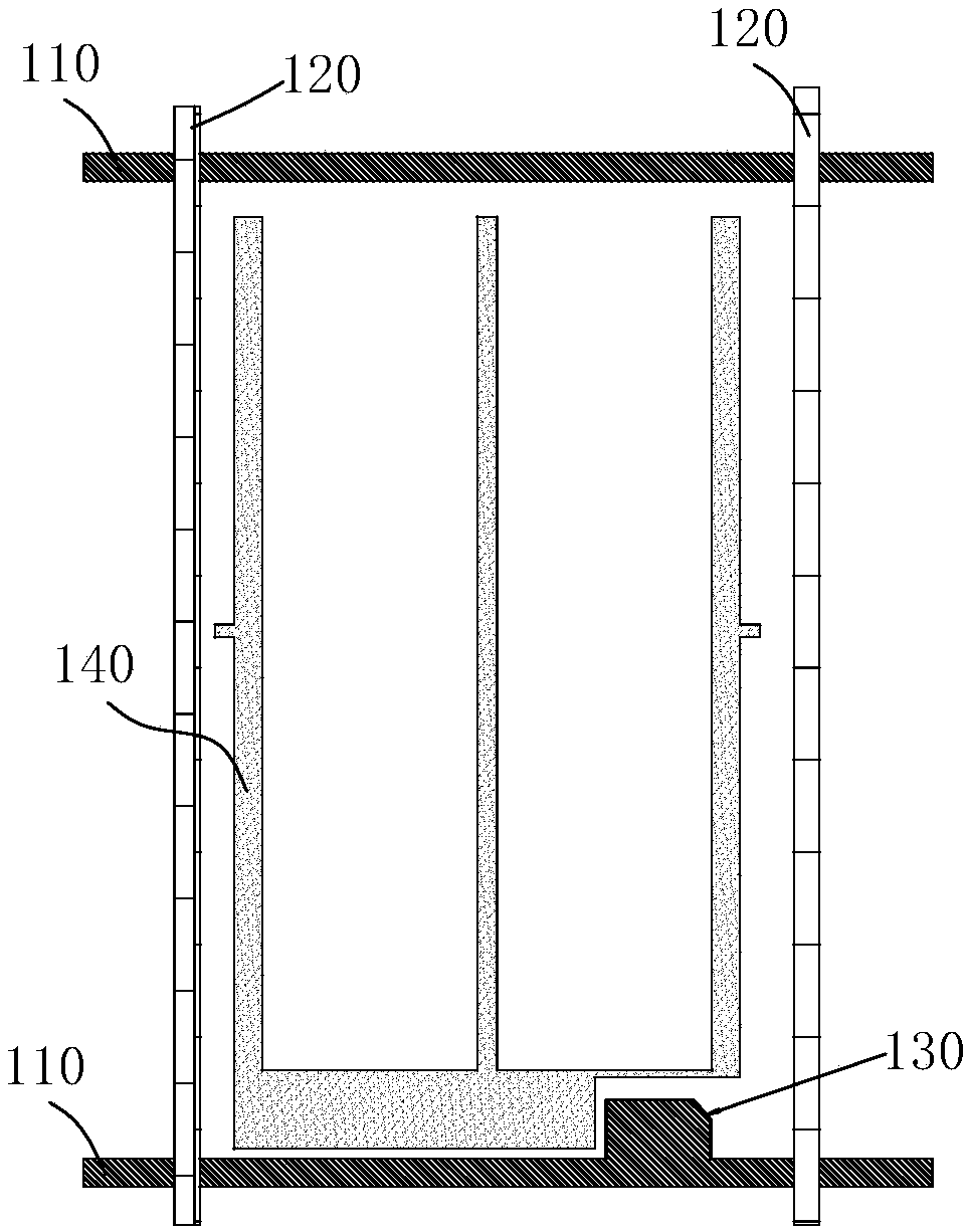
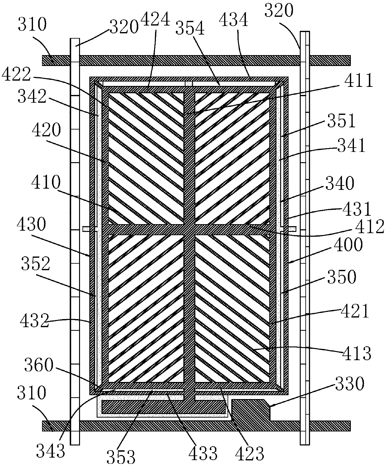
The embodiment of the invention discloses a pixel structure, which comprises a scanning line, a data line, a pixel driving appliance, and a public electrode. The data line and the scanning line are intersected mutually to define a pixel unit, and the pixel unit comprises a pixel electrode; the pixel electrode comprises a main body part and a rim part, and the rim part is arranged around the main body part and electrically connected with the main body part; the public electrode is in a heterosphere structure with the pixel electrode, and the public electrode and the pixel electrode are formed to be a storage capacitor; the public electrode comprises a peripheral part neighbored to the data line or / and the scanning line, wherein the pixel electrode further comprises an extending part locatedat the outside of the rim part, and the extending part is electrically connected with the rim part and an avoiding hole is formed between the extending part and the rim part; the peripheral part of the public electrode is corresponding to the avoiding hole. The embodiment of the invention further discloses a liquid crystal display panel. The pixel structure and the liquid crystal display panel have the advantages of improving the volume of the storage capacitor and improving stray capacitance and dark fringe.

Description

technical field [0001] The invention relates to the field of display technology, in particular to a pixel structure and a liquid crystal display panel. Background technique [0002] Liquid crystal display (LCD, liquid Crystal Display) is one of the most widely used flat-panel displays, and there are many modes for realizing its image display, such as TN (twisted nematic liquid crystal, twisted nematic liquid crystal) mode, IPS (In Plane Switching liquid crystal, in-plane switching liquid crystal) mode and VA (VerticalAlignment liquid crystal, vertical alignment liquid crystal) mode. [0003] As a branch mode in the VA mode, HVA adopts the method of photo-alignment and charging to realize the curing of a liquid crystal layer with a certain pre-tilt angle on the surface of PI, so as to omit the traditional rubbing alignment. [0004] In order to realize the wide viewing angle of the liquid crystal display, the pixel electrode in the HVA mode adopts a multi-domain (Muti-Domain...

Claims


Application Information

Patent Timeline
IPC IPC(8): G02F1/1343G02F1/1362
CPCG02F1/136213G02F1/134309G02F1/13606G02F1/136218G02F1/136286G02F1/1368G02F2201/121G02F2201/123G09G3/3677G09G3/3688G09G2300/0426G09G2300/0439
Inventor 叶岩溪
Owner SHENZHEN CHINA STAR OPTOELECTRONICS SEMICON DISPLAY TECH CO LTD
Learn More