Making method of OLED backplane

A manufacturing method and backplane technology, applied in semiconductor/solid-state device manufacturing, electrical components, electrical solid-state devices, etc., can solve problems such as increased interface defects, reduced device mobility, and poor conductivity, to reduce interface defects , Improve stability, improve conductivity

Active Publication Date: 2018-01-19
SHENZHEN CHINA STAR OPTOELECTRONICS SEMICON DISPLAY TECH CO LTD
View PDF6 Cites 13 Cited by
  • Summary
  • Abstract
  • Description
  • Claims
  • Application Information

AI Technical Summary

Problems solved by technology

[0006] In oxide semiconductor thin film transistors, the oxygen content in the active layer (i.e., oxide semiconductor layer) has a great influence on device characteristics. Currently, the active layer in oxide semiconductor thin film transistors generally adopts a single-layer design. The active layer of a single film layer is formed by one-time deposition. If the oxygen flow rate is large during deposition, the oxygen content in the active layer will be too high, the conductivity will be deteriorated, and the mobility of the device will be reduced; and if the oxygen flow rate during deposition If it is smaller, the oxygen content in the active layer will be too low, and the oxygen vacancies will be too many, resulting in the increase of interface defects at the contact interface between the active layer and the buffer layer and the contact interface between the active layer and the gate insulating layer. , the device stability deteriorates

Method used


Image

  • Making method of OLED backplane
  • Making method of OLED backplane
  • Making method of OLED backplane

Examples


Embodiment Construction

[0049] In order to further illustrate the technical means adopted by the present invention and its effects, the following describes in detail in conjunction with preferred embodiments of the present invention and accompanying drawings.

[0050] see Figure 13 , the invention provides a method for manufacturing an OLED backplane, comprising the following steps:

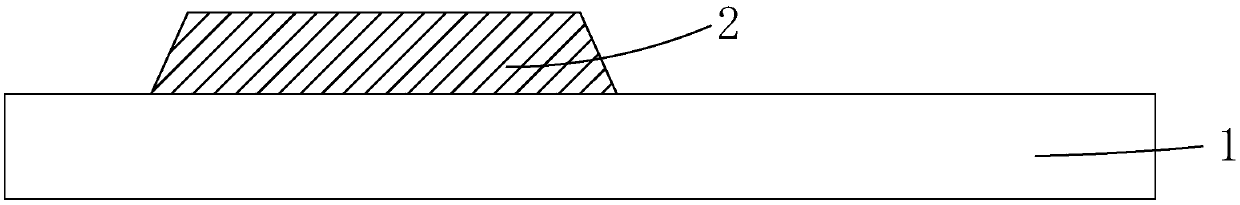
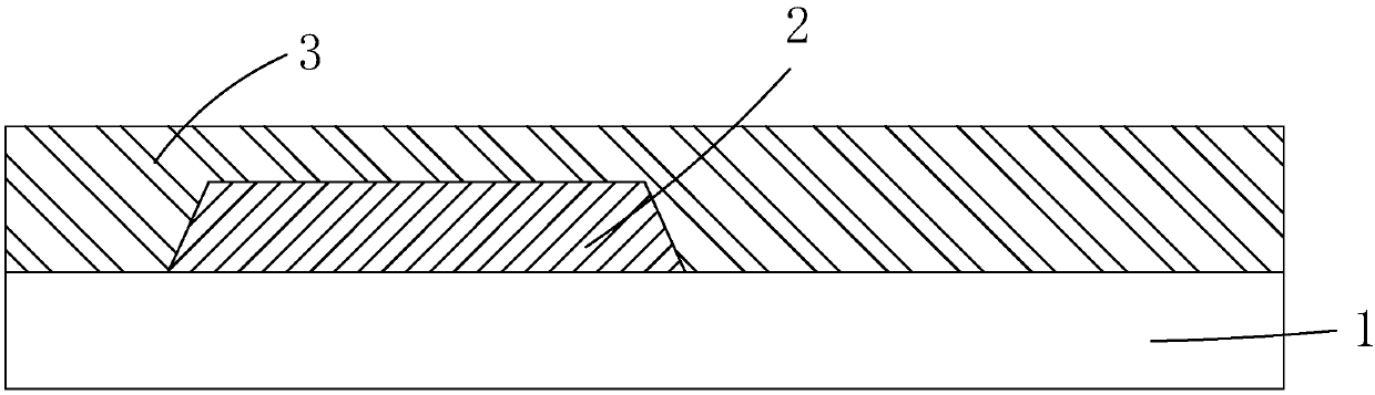
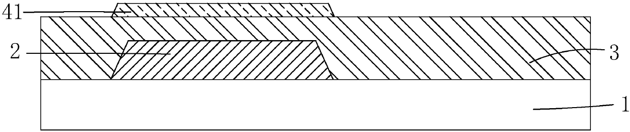
[0051] Step S1, please refer to figure 1 and figure 2 , providing a base substrate 1 on which a buffer layer 3 is formed.

[0052] In specific implementation, such as figure 1 As shown, the step S1 may further include: depositing a light-shielding metal film on the base substrate 1, patterning the light-shielding metal film, and forming a light-shielding layer 2 corresponding to the area where the active layer 4 is to be formed. The buffer layer 3 covers the light-shielding layer 2 and the base substrate 1, and the light-shielding layer 2 is used to shield the subsequently formed active layer 4, so as to prevent t...


PUM


Abstract

The invention provides a making method of an OLED backplane, which is characterized in that an active layer of a film transistor is made by successively depositing a first oxide semiconductor layer, asecond oxide semiconductor layer, and a third oxide semiconductor layer; a flow ratio of argon and oxide input when the first oxide semiconductor layer and the third oxide semiconductor layer depositis larger than a flow ratio of argon and oxide input when the second oxide semiconductor layer deposits; an oxygen content of the first oxide semiconductor layer and the third oxide semiconductor layer is larger than an oxygen content of the second oxide semiconductor layer; thereby conductivity of the active layer of the film transistor device is increased, the interface defects are reduced, andstability of the film transistor device is improved.

Description

technical field [0001] The invention relates to the field of display technology, in particular to a method for manufacturing an OLED backplane. Background technique [0002] Flat-panel display devices have many advantages such as thin body, power saving, and no radiation, and have been widely used. Existing flat panel display devices mainly include liquid crystal display devices (Liquid Crystal Display, LCD) and organic light emitting diode display devices (Organic Light Emitting Display, OLED). [0003] Organic light-emitting diode display devices have excellent characteristics such as self-illumination, no need for backlight, high contrast, thin thickness, wide viewing angle, fast response speed, flexible panels, wide operating temperature range, and simple structure and manufacturing process. It is considered as an emerging application technology for the next generation of flat panel displays. OLED display devices generally include: a substrate, an anode disposed on the...

Claims


Application Information

Patent Timeline
Patent Type & Authority Applications(China)
IPC IPC(8): H01L21/77H01L27/12H01L27/32
CPCH01L21/02631H01L21/02565H01L21/02488H01L21/02491H01L21/02505H01L21/02483H01L29/7869H01L29/78696H01L29/66969H01L29/78633H01L27/1225H10K59/126H01L27/1259H10K59/1201H01L21/02164H01L21/0217H01L21/383H01L21/443H01L21/47573H01L27/127H01L29/24H10K59/1213H10K50/81H10K50/82H10K59/122H10K71/00
Inventor 刘方梅
Owner SHENZHEN CHINA STAR OPTOELECTRONICS SEMICON DISPLAY TECH CO LTD
Why Eureka
Try Eureka