Eureka AIR delivers breakthrough ideas for toughest innovation challenges, trusted by R&D personnel around the world.

E-fuse (electrically programmable fuse) structure of semiconductor device

An electric programming fuse and semiconductor technology, which is applied in the direction of instruments, static memory, read-only memory, etc., can solve the problems of decoder signal selection and signal direction not clear enough, layout layout not symmetrical and uniform, and power supply and ground not being able to form a loop, etc. , to achieve the effect of superior performance, clear layout and smooth signal

Inactive Publication Date: 2018-01-26
SHANGHAI HUALI MICROELECTRONICS CORP
View PDF6 Cites 0 Cited by
  • Summary
  • Abstract
  • Description
  • Claims
  • Application Information

AI Technical Summary

Problems solved by technology

figure 1 The layout of the medium layout is not symmetrical and uniform, the signal selection and direction of the decoder are not clear enough, and the power supply ground cannot be looped to supply internal power, indicating that there is still room for improvement in the performance of this layout.

Method used


Image

  • E-fuse (electrically programmable fuse) structure of semiconductor device
  • E-fuse (electrically programmable fuse) structure of semiconductor device

Examples


Embodiment Construction

[0019] Specific embodiments of the present invention are given below in conjunction with the accompanying drawings, but the present invention is not limited to the following embodiments. The advantages and features of the present invention will become apparent from the following description and claims. It should be noted that, the accompanying drawings are all in a very simplified form and use inaccurate ratios, and are only used for the purpose of assisting in explaining the embodiments of the present invention conveniently and clearly.

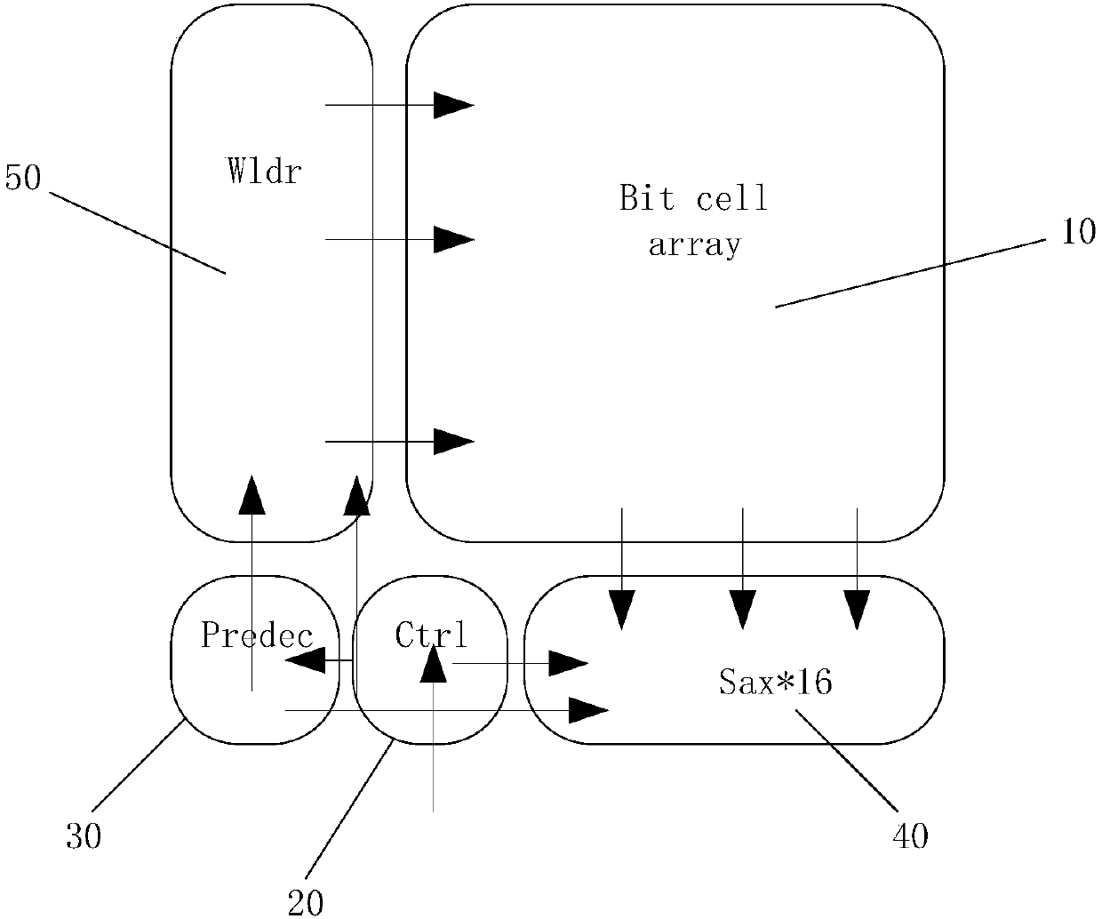
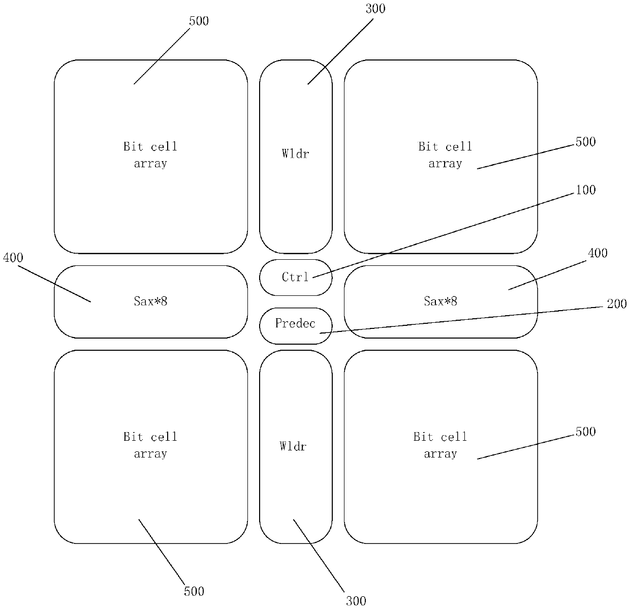
[0020] Please refer to figure 2 , figure 2 Shown is a schematic diagram of the layout structure of the E-fuse according to the preferred embodiment of the present invention. The present invention proposes an electrical programming fuse structure for a semiconductor device, including: a control module 100 (Ctrl) and a pre-decoder module 200 (Predec); a word line driver module 300 (Wldr), which is arranged in the control module 100 and Th...


PUM


Abstract

The invention provides an E-fuse (electrically programmable fuse) structure of a semiconductor device. The E-fuse structure comprises a control module, a pre-decoder module, word line drive modules, Sax modules and four bit cell arrays, wherein the word line drive modules are arranged on upper and lower sides of the control module and the pre-decoder module; the Sax modules are arranged on left and right sides of the control module and the pre-decoder module; the two word line drive modules and the two Sax modules form a cross-shaped structure; the four bit cell arrays are symmetrically distributed according to the cross-shaped structure. According to the E-fuse structure of the semiconductor device, an E-fuse territory with clear layout, smooth signals and excellent performance is provided, large bit cell arrays are symmetrically distributed vertically and bilaterally, power supply ground buses are distributed on the periphery to form a loop, logic selection circuits are distributed in the loop, signal selection of decoders and symmetry of the arrays are both better improved, and thus, the performance of the E-fuse is improved.

Description

technical field [0001] The invention relates to the field of layout design of CMOS integrated circuits, and in particular to an electrical programming fuse structure of a semiconductor device. Background technique [0002] In the field of integrated circuits, fuses refer to some connection lines formed in integrated circuits that can be blown. Initially, fuses are used to connect redundant circuits in integrated circuits. Once the integrated circuits are found to be defective, the fuses are used to repair or replace the defective circuits. The fuse is generally a laser fuse (Laser Fuse) and an electrically programmable fuse (Electrically Programmable Fuse, hereinafter referred to as E-fuse). With the development of semiconductor technology, E-fuse gradually replaced the laser fuse. [0003] Currently, electrical programming fuse structures (E-fuses) are mostly used in semiconductor devices, and the one-time electrical programming fuses of E-fuse are widely used because of ...

Claims


Application Information

Patent Timeline
IPC IPC(8): G11C17/18G11C17/16
Inventor 伍苹
Owner SHANGHAI HUALI MICROELECTRONICS CORP
Why Eureka
Eureka Blog
Learn More