Ultrasonic-welding joining apparatus of semiconductor substrate

An ultrasonic welding and bonding device technology, which is applied in semiconductor devices, semiconductor/solid-state device manufacturing, semiconductor/solid-state device components, etc., can solve problems such as physical vibration or weak weld cracks, reduced joint quality, and reduced productivity. Achieve the effects of improving joint quality, preventing the generation of environmental pollutants, and improving productivity

Active Publication Date: 2018-01-26
JMJ KOREA CO LTD
View PDF4 Cites 6 Cited by
  • Summary
  • Abstract
  • Description
  • Claims
  • Application Information

AI Technical Summary

Problems solved by technology

[0003] However, as described above, when the lead frame 160 is bonded to the copper-clad ceramic substrate 10 by soldering, it is vulnerable to physical vibration or cracks in the solder joint, and the quality of the joint decreases, resulting in extremely low productivity and the occurrence of lead or harmful substances. Environmental pollutants such as gas

Method used


Image

  • Ultrasonic-welding joining apparatus of semiconductor substrate
  • Ultrasonic-welding joining apparatus of semiconductor substrate
  • Ultrasonic-welding joining apparatus of semiconductor substrate

Examples


Embodiment Construction

[0086] Hereinafter, the structure and operation of the ultrasonic welding and bonding device for semiconductor substrates according to the present invention will be described in detail with reference to the drawings and preferred embodiments.

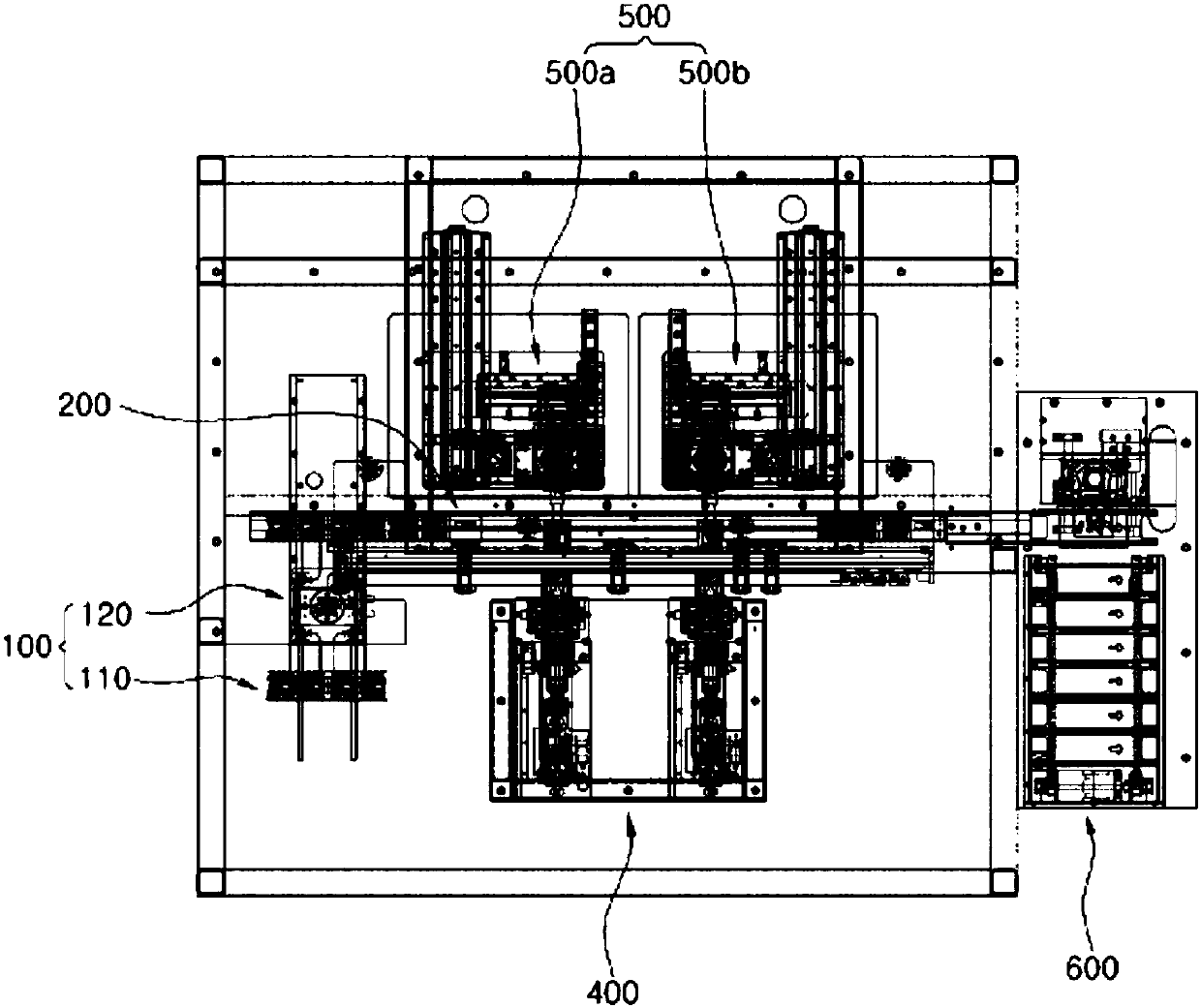
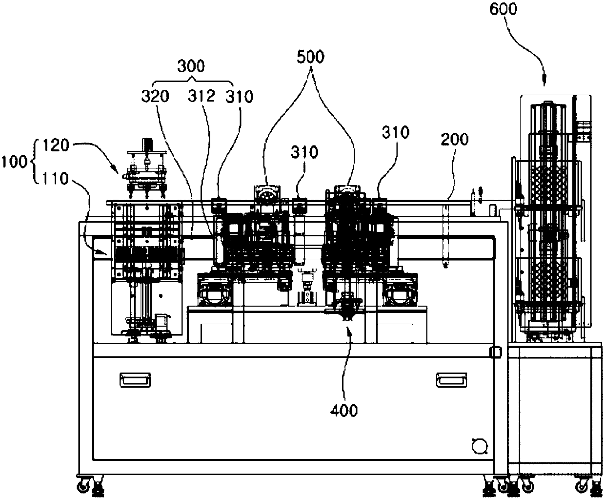
[0087] Such as figure 2 and image 3 As shown, the ultrasonic welding bonding apparatus of the present invention includes a lead frame loading unit 100 , an index rail 200 , a lead frame transfer unit 300 , a substrate loading unit 400 , an ultrasonic welding unit 500 and an unloading unit 600 .

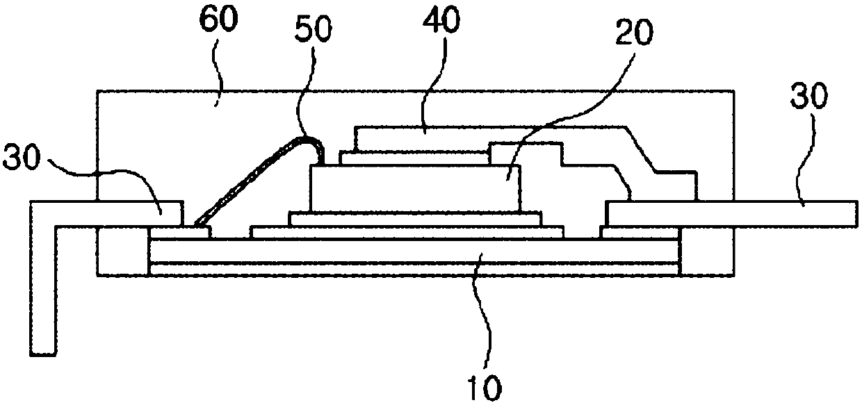
[0088] Such as Figure 4 As shown, the lead frame loader 100 is a part for automatically feeding the lead frame LF bonded to the copper-clad ceramic substrate S, and includes a stack loader 110 and a separator 120 .

[0089] The stack loader 110 lifts and moves a plurality of lead frames LF in a multi-layered state, and supplies them to the separator 120 . Such as Figure 4 As shown, the above-mentioned stack loader 110 includes: a motor ...


PUM


Abstract

The invention discloses an ultrasonic-welding joining apparatus of a semiconductor substrate. The present invention relates to an ultrasonic-welding joining apparatus and, more particularly, to an apparatus for joining, using ultrasonic welding, a lead frame on a DBC substrate of a semiconductor package. The ultrasonic-welding joining apparatus according to the present invention comprises: a lead-frame loading part for supplying a lead frame; a substrate loading part for supplying a DBC substrate; an index rail in which the DBC substrate and the lead frame are seated; an ultrasonic-welding part for joining, using ultrasonic welding, the lead frame and the DBC substrate seated in the index rail; and an unloading part for carrying out the lead frame and the DBC substrate joined by the ultrasonic-welding part.

Description

technical field [0001] The present invention relates to an ultrasonic welding bonding apparatus, and more particularly, to an apparatus for bonding a lead frame to a copper-clad ceramic substrate of a semiconductor package by ultrasonic welding. Background technique [0002] Usually, such as figure 1 As shown, the semiconductor chip package for power using a copper-clad ceramic substrate includes a copper-clad ceramic substrate 10, a semiconductor chip 20, a lead frame 30, and a housing body 60, and the lead frame 160 is bonded to the copper-clad ceramic substrate 10 by an adhesive such as welding. The copper pattern is electrically connected to the semiconductor chip 20 through the conductive clip 40 or the bonding wire 50 . [0003] However, as described above, when the lead frame 160 is bonded to the copper-clad ceramic substrate 10 by soldering, it is vulnerable to physical vibration or cracks in the solder joint, and the quality of the joint decreases, resulting in ext...

Claims


Application Information

Patent Timeline
Patent Type & Authority Applications(China)
IPC IPC(8): H01L21/48H01L21/677H01L23/00H01L23/495
CPCH01L2924/181H01L2224/40245H01L21/48H01L2224/48091H01L2224/48247H01L23/3735H01L23/49524H01L23/49562H01L21/67144H01L2224/73263H01L2224/73265H01L2924/00014B23K20/10H05K13/0465H01L2224/291B23K2101/36H01L2224/73221H01L2924/00012H01L2224/84801H01L2224/37099H01L2224/83801H01L2924/014H01L2924/00
Inventor 崔伦华李仁燮赵廷太崔淳性
Owner JMJ KOREA CO LTD
Why Eureka
Try Eureka