Nanofiber substrate as well as preparation method of nanofiber substrate and applications of nanofiber substrate
A nanofiber and substrate technology, applied in the field of biomedical materials, can solve the problems of CTC purity and low biological activity
- Summary
- Abstract
- Description
- Claims
- Application Information
AI Technical Summary
Problems solved by technology
Method used
Image
Examples
Embodiment 1
[0072] Step 1: Prepare a glass substrate.
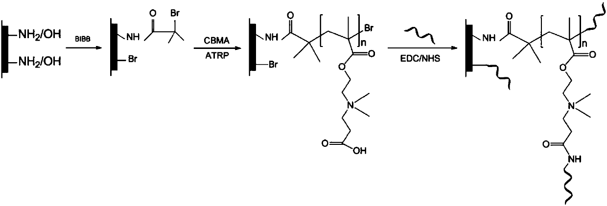
[0073] Step 2: Depositing a nanostructure layer on a glass substrate. Specifically: build an electrospinning device, which includes a high-voltage power supply, a micro-injection pump, a 5mL disposable syringe, and a receiving station; transfer the electrospinning solution prepared in the preparation example to a 5mL disposable syringe, and the syringe Use 5-7# needles for the needle, adjust the distance between the receiving station and the needle of the syringe to 10-18cm, adjust the voltage of the high-voltage power supply to 15-24kV, place the glass substrate on the receiving station, connect the high-voltage power supply, The injector is jet-spun to the receiving station, and the time of controlling the injector jet-spinning is 2min, so that a nanostructure layer with a thickness of no more than 200-300nm is produced, and the nanostructure layer is connected on the glass substrate, and the nanostructure layer is made of Chitosa...
Embodiment 2
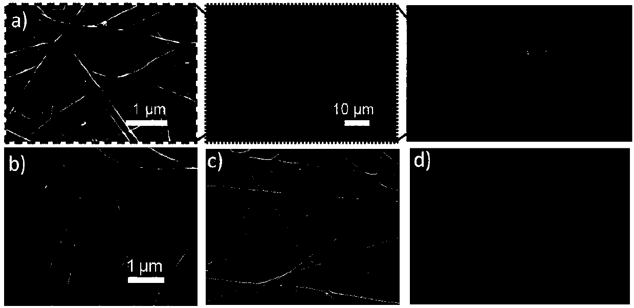
[0082] The difference between this embodiment and Embodiment 1 is that in step 2 of this embodiment, the injection spinning time of the injector is controlled to be not less than 8 minutes, and a nanostructure layer with a thickness of not less than 5-10 μm is obtained, so that the nanostructure layer attached to a glass substrate. Other preparation steps are the same as in Example 1, and the nanofiber substrate prepared in this example is named JD-2. Such as figure 1 a) and figure 1 Shown in b), be the macrophotograph and the SEM image of the chitosan nanofibers that make in the present embodiment, wherein, figure 1 a) From right to left, respectively, the macrophotograph, the SEM image at 10 μm and the SEM image at 1 μm of the chitosan nanofibers prepared in this example.
PUM
| Property | Measurement | Unit |
|---|---|---|
| diameter | aaaaa | aaaaa |
| thickness | aaaaa | aaaaa |
| thickness | aaaaa | aaaaa |
Abstract
Description
Claims
Application Information


