
Manufacturing method of BGA partial pad gold plating for PCB

A local soldering and pad technology, which is applied in chemical/electrolytic methods to remove conductive materials, reinforce conductive patterns, and print circuit secondary treatment. problem, achieve the effect of improving the bonding force of the coating and being easy to dispose of

Active Publication Date: 2018-01-30
SHENNAN CIRCUITS
View PDF7 Cites 11 Cited by
  • Summary
  • Abstract
  • Description
  • Claims
  • Application Information

AI Technical Summary

Problems solved by technology

[0004] This solution requires continuous processing of copper immersion and electroplating, and the thickness of the electroplated copper layer needs to be >0.005mm, otherwise the bonding force of the plating layer is very poor, and the nickel and gold in the subsequent electroplating are easy to fall off
However, the thickness of electroplated copper exceeds 0.005mm, and it is difficult to micro-etch it off in the post-process
Moreover, due to the existence of line gaps, some graphics or through holes that do not need to be plated may be plated with copper

Method used


Image

  • Manufacturing method of BGA partial pad gold plating for PCB
  • Manufacturing method of BGA partial pad gold plating for PCB
  • Manufacturing method of BGA partial pad gold plating for PCB

Examples


Embodiment Construction

[0020] In order to enable those skilled in the art to better understand the solutions of the present invention, the following will clearly and completely describe the technical solutions in the embodiments of the present invention in conjunction with the drawings in the embodiments of the present invention. Obviously, the described embodiments are only It is an embodiment of a part of the present invention, but not all embodiments. Based on the embodiments of the present invention, all other embodiments obtained by persons of ordinary skill in the art without making creative efforts shall fall within the protection scope of the present invention.

[0021] The terms "first", "second", "third" and the like in the description and claims of the present invention and the above drawings are used to distinguish different objects, rather than to describe a specific order. Furthermore, the terms "include" and "have", as well as any variations thereof, are intended to cover a non-exclus...


PUM

PropertyMeasurementUnit
lengthaaaaaaaaaa
thicknessaaaaaaaaaa

Abstract

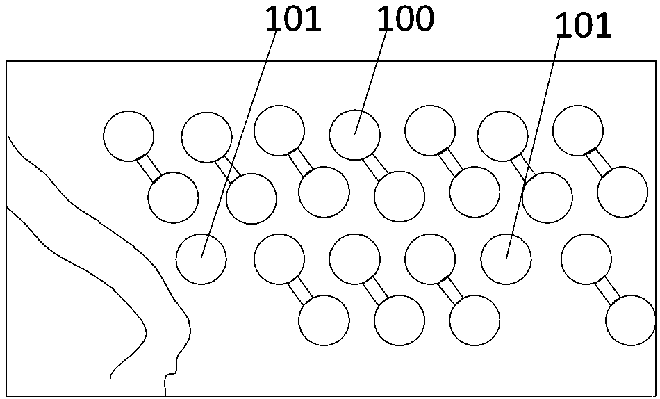
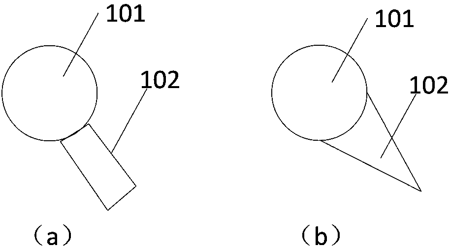
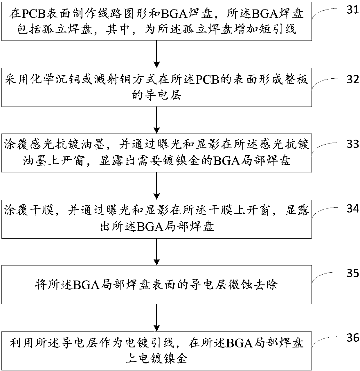
The invention discloses a manufacturing method of BGA partial pad gold plating for a PCB. The manufacturing method comprises the steps of manufacturing a circuit pattern and a BGA ad on the surface ofthe PCB, wherein the BGA pad comprises an isolated pad; adding a short lead to the isolated pad; forming a conductive layer of the whole plate on the surface of the PCB by adopting a chemical copperdeposition or sputtering mode; coating a photosensitive anti-plating ink on the surface of the PCB; windowing on the photosensitive anti-plating ink through exposure and development to expose a BGA partial pad requiring nicke-gold plating; continuously coating a dry film on the surface of the PCB; windowing in the dry film through exposure and development to expose the BGA partial pad; microetching and removing the conductive layer on the surface of the BGA partial pad; and plating nickel-gold on the BGA partial pad. The problem of nickel-gold plating of an isolated pad is solved, the bondingforce of a plating layer can be improved, and the nickel-gold can be prevented from falling.

Description

technical field [0001] The invention relates to the technical field of PCB production, in particular to a production method for BGA partial pad gold plating of PCB. Background technique [0002] BGA (Ball Grid Array, solder ball array package) pads designed on PCB (Printed Circuit Board, printed circuit board) usually need to be electroplated with nickel gold, and these BGA pads may include isolated pads, isolated pads and other The lines are not connected and cannot be directly plated. [0003] For such PCBs, the process of electroplating nickel and gold is generally: chemically deposit copper on the PCB, and then electroplate to form a uniform and dense copper layer on the surface as a conductive layer, and use the formed conductive layer as an electroplating layer. Leads, for BGA pads that require nickel-gold plating, including isolated pads, electroplate nickel-gold, and then micro-etch to remove the conductive layer after electroplating. The patent document No. 200610...

Claims


Application Information

Patent Timeline
Patent Type & Authority Applications(China)
IPC IPC(8): H05K3/24H05K3/06
Inventor 幸锐敏杨洲钱文鲲缪桦
Owner SHENNAN CIRCUITS
Learn More