

Method for manufacturing base material having gold-plated metal fine pattern, base material having gold-plated metal fine pattern, printed wiring board, interposer, and semiconductor device
- Summary
- Abstract
- Description
- Claims
- Application Information
AI Technical Summary
Benefits of technology
Problems solved by technology
Method used
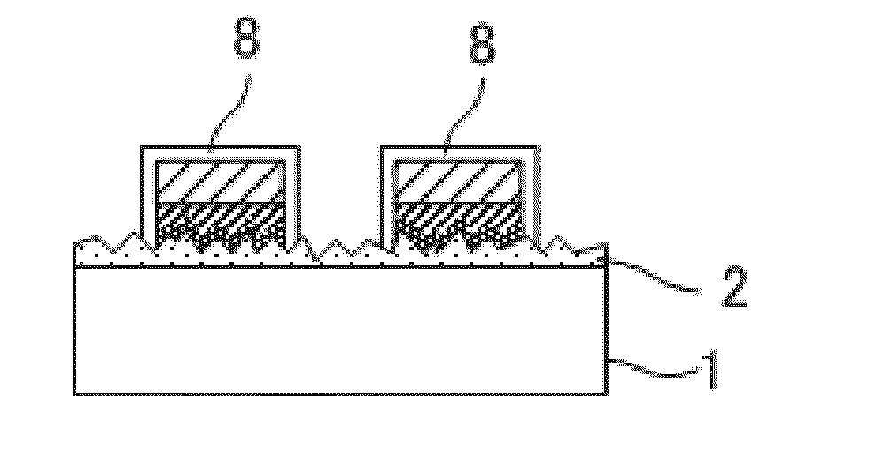
Image

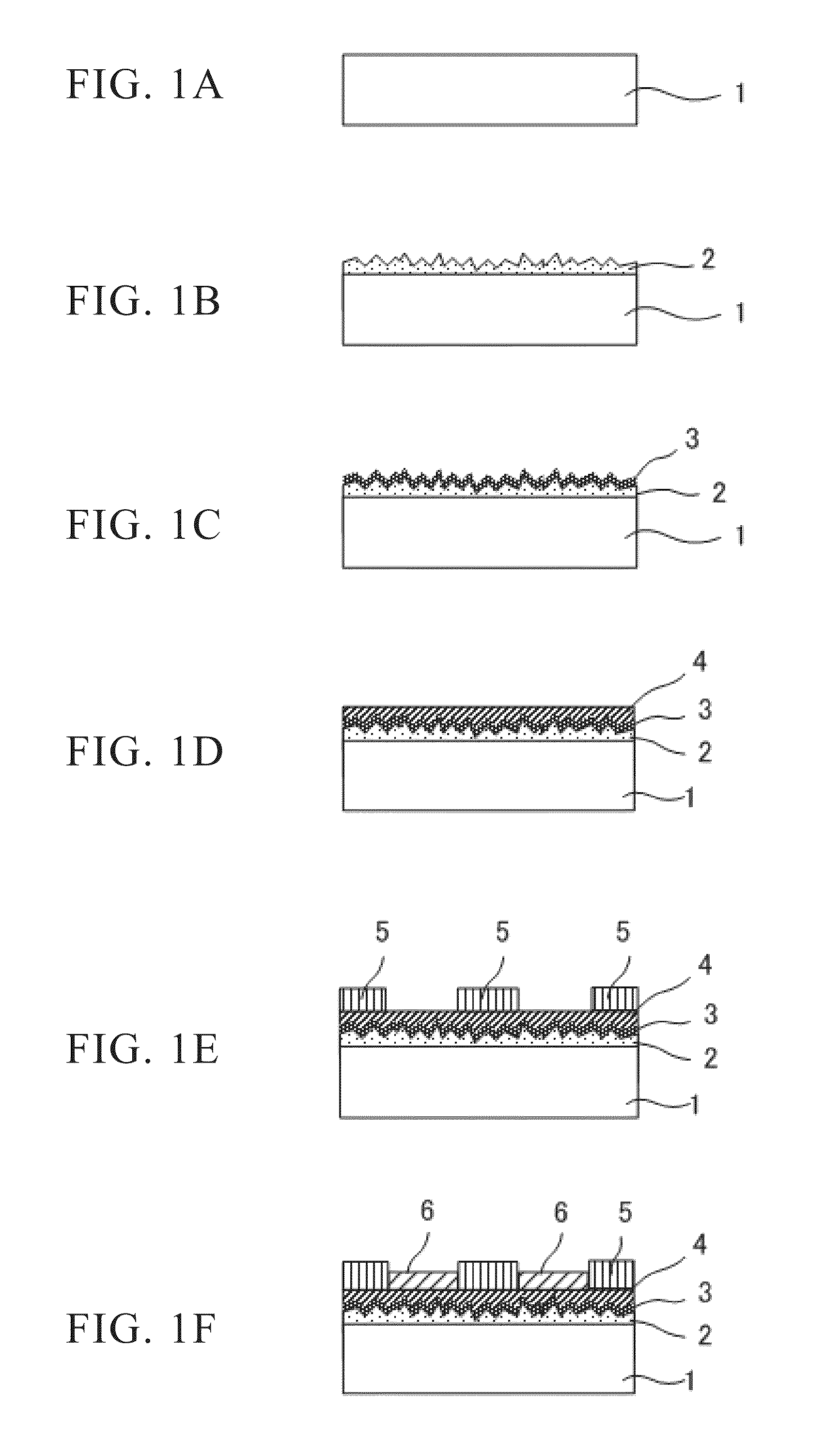
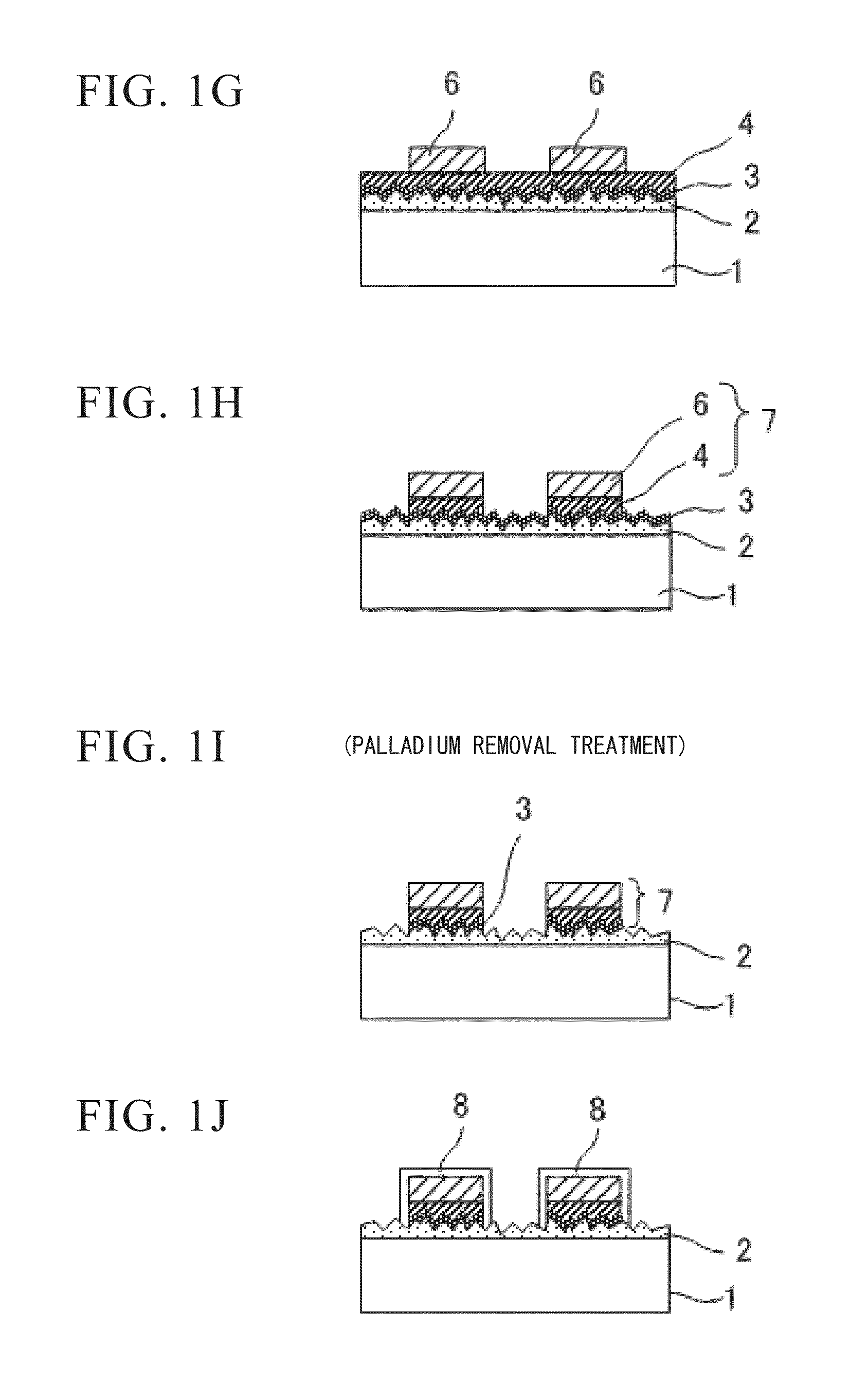
Examples
example 1
Treatment (a), ENEPIG Step
1. Preparation of Primer Resin
[0215]31.5 parts by weight of a methoxynaphthalenearalkyl type epoxy resin (EPICLON HP-5000, manufactured by DIC Corporation,) as an epoxy resin, 26.7 parts by weight of a phenol novolak type cyanate resin (Primaset PT-30, manufactured by Lonza Inc.) as a cyanate ester resin, 31.5 parts by weight of a polyamide resin (KAYAFLEX BPAM01, manufactured by Nippon Kayaku Co., Ltd.) and 0.3 part by weight of imidazole (CUREZOL 1B2PZ, manufactured by Shikoku Chemical Corporation) as a curing catalyst were dissolved by stirring in a mixed solvent of dimethylacetamide and methyl ethyl ketone for 30 minutes. Furthermore, 0.2 part by weight of an epoxysilane-coupling agent (A187, manufactured by Nippon Unicar Company Limited) as a coupling agent and 9.8 parts by weight of spherical fused silica (SP-7 having an average particle size of 0.75 μm, manufactured by Fuso Chemical Co., Ltd.) as an inorganic filler were added, followed by stirring f...
example 2
Treatment (b), ENEPIG Step
[0232]In the surface treatment step of Example 1, a surface treatment using a chemical liquid containing nitric acid and chlorine ions was not carried out, and a test piece was dipped in a KCN-containing liquid having a concentration of 20 g / liter at a liquid temperature of 25° C. for 1 minute, and then washed three times with water (treatment with KCN).
example 3
Treatment (c), ENEPIG Step
[0233]In the surface treatment step of Example 1, a surface treatment using a chemical liquid containing nitric acid and chlorine ions was not carried out, and a desmear treatment with a chemical liquid (surface treatment with a sodium permanganate-containing liquid) was carried out by the procedure shown below.
(1) Resin Surface Swelling Treatment
[0234]A test piece was dipped in a mixed liquid (pH 12) of commercially available sodium hydroxide and an ethylene glycol-based solvent-containing liquid (Swelling Dip Securiganth P liquid for initial make-up of electrolytic bath, manufactured by Atotech Japan K.K.) at a liquid temperature of 60° C. for 2 minutes, and then washed three times with water.
(2) Resin Surface Roughening Treatment
[0235]A test piece was dipped in a sodium permanganate-containing roughening treatment liquid (Concentrate Compact CP liquid for initial make-up of electrolytic bath, manufactured by Atotech Japan K.K.) at a liquid temperature of...
PUM
| Property | Measurement | Unit |
|---|---|---|
| Length | aaaaa | aaaaa |
| Length | aaaaa | aaaaa |
| Length | aaaaa | aaaaa |
Abstract
Description
Claims
Application Information