Chip with high conductivity

A high-conductivity, chip technology, applied in circuits, electrical components, electrical solid devices, etc., to achieve excellent electrical conductivity, stable thermal conductivity, and a wide range of applicable temperatures.

Inactive Publication Date: 2018-02-02
俞亮亮
View PDF0 Cites 0 Cited by
  • Summary
  • Abstract
  • Description
  • Claims
  • Application Information

AI Technical Summary

Problems solved by technology

The substrate can be an existing chip or silicon wafer or wafer etc.

Method used


Image

  • Chip with high conductivity

Examples


Embodiment Construction

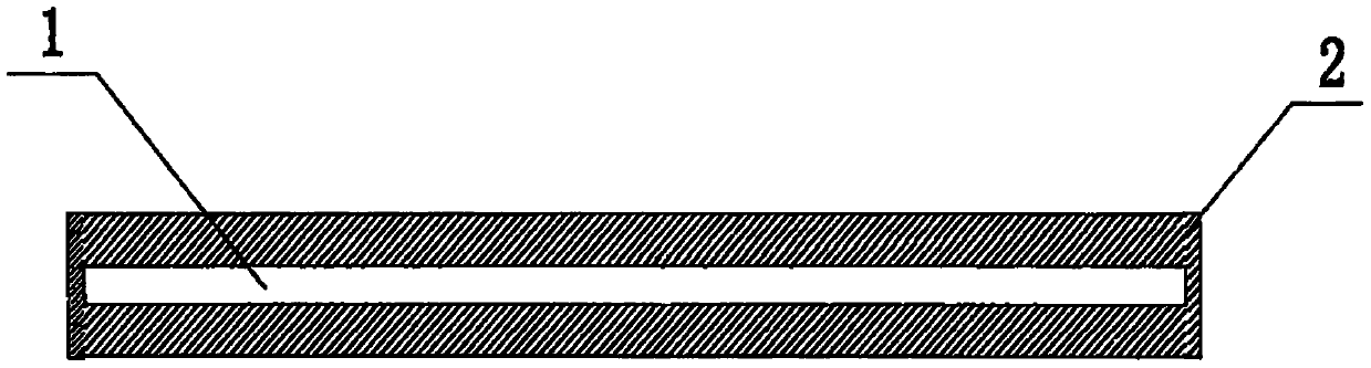
[0010] A chip with high conductivity includes a substrate 1, and a conductive layer 2 outside the substrate 1.

[0011] The conductive layer 2 is a nano-diamond layer. The nano-diamond layer is formed by uniformly spreading nano-diamond paste on the substrate 1 .

[0012] The thickness of the nanodiamond layer is 1-3 nanometers.

[0013] The substrate 1 has a thickness of 1.5-2.5 mm.

[0014] Nano-diamond paste is a new type of material, generally gray paste, with a thermal conductivity of 4.7w / m K and a dielectric constant of 14.5at1MHz. In addition to the general properties of diamonds, nano-diamond paste also has many properties of nano-materials, such as non-toxicity, small size effect, surface / interface effect, quantum size effect, macroscopic quantum tunneling effect, and has a very broad application prospect. However, the biggest problem facing the application and research of nanodiamonds at present is to solve the deagglomeration of hard aggregates and the stable di...


PUM

PropertyMeasurementUnit
thicknessaaaaaaaaaa
thicknessaaaaaaaaaa
thermal conductivityaaaaaaaaaa

Abstract

The invention provides a chip with high conductivity. The chip comprises a substrate, wherein a conductive layer is arranged outside the substrate. According to the chip with high conductivity, a conductive and heat-conducting nano-diamond layer is arranged outside the chip, so that a silicon wafer has excellent thermal efficiency and conductive efficiency, the thermal conductivity can reach 4.7W/m.K and manufacturing is simple; and the used nano-diamond paste does not have corrosivity and oxidation resistance, and the curing phenomenon is not easy to occur. Therefore, the chip with high conductivity is relatively wide in applicable temperature range and stable in heat conduction effect, and can be widely used as LED wafer, a photovoltaic polysilicon wafer and various cooling interface chips.

Description

technical field [0001] The invention relates to a chip, in particular to a chip with high electrical conductivity. Background technique [0002] The silicon chip used in the chip has the physical properties of a metalloid, has weak conductivity, and its conductivity increases with the increase of temperature. Generally, in order to improve the conductivity, a trace amount of group IIIA elements, such as boron, can be added to form a p-type silicon semiconductor in silicon wafer production; or a trace amount of group VA elements, such as phosphorus or arsenic, can also be added It can improve the degree of conductivity and form n-type silicon semiconductor. However, silicon wafers with higher conductivity are required in various application fields of silicon wafers, but the manufacturing cost of chips with high conductivity is high and the manufacturing process is complicated. Contents of the invention [0003] The object of the present invention is to provide a chip with...

Claims


Application Information

Patent Timeline
Patent Type & Authority Applications(China)
IPC IPC(8): H01L23/29H01L23/373H01L23/492
CPCH01L23/29H01L23/3732H01L23/4928
Inventor 俞亮亮
Owner 俞亮亮
Why Eureka
Try Eureka