Photoetching-etching technological method of top select gate cut

A process method and selection gate technology, applied in the direction of electrical components, electrical solid devices, circuits, etc., can solve the problems of difficulty in controlling the uniformity of key dimensions, complex and cumbersome processes and equipment, and increased manufacturing costs, so as to reduce the key to lithography. size, the effect of reducing the critical dimension

Inactive Publication Date: 2018-02-02
YANGTZE MEMORY TECH CO LTD
View PDF5 Cites 5 Cited by
  • Summary
  • Abstract
  • Description
  • Claims
  • Application Information

AI Technical Summary

Problems solved by technology

[0013] Although in the prior art it is also possible to use an immersion tool (Immersion Tool) to achieve a photolithography critical dimension (Ph CD) as short as 80 nm or below on a single-layer mask with 193 nm immersion stepping technology, but doing so will The following problems are caused: on the one hand, the use of immersion tools (Immersion Tool) will make the entire process and equipment more complicated and cumbersome, which will undoubtedly increase the preparation cost; Small and critical dimension uniformity (CD Uniformity) is difficult to control

Method used


Image

  • Photoetching-etching technological method of top select gate cut
  • Photoetching-etching technological method of top select gate cut
  • Photoetching-etching technological method of top select gate cut

Examples


Embodiment Construction

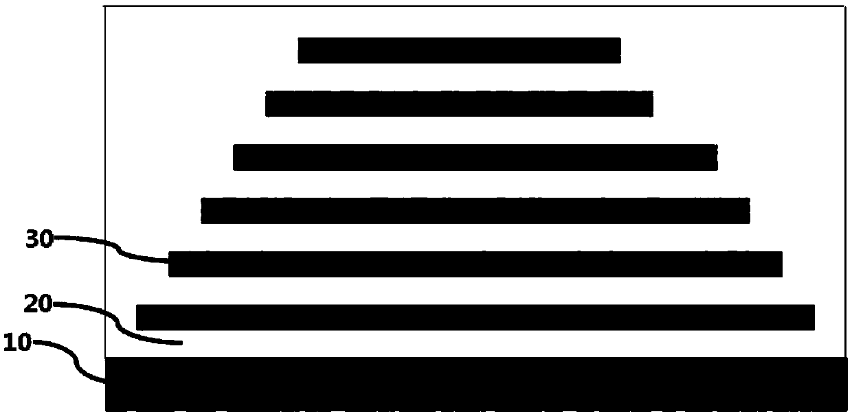
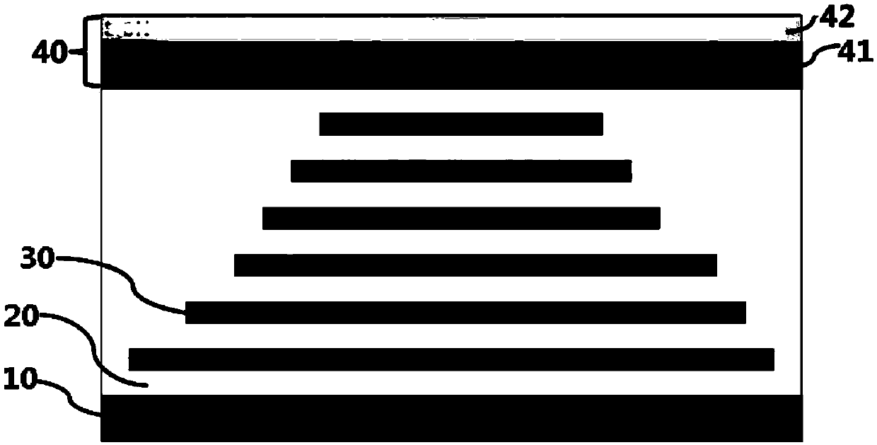
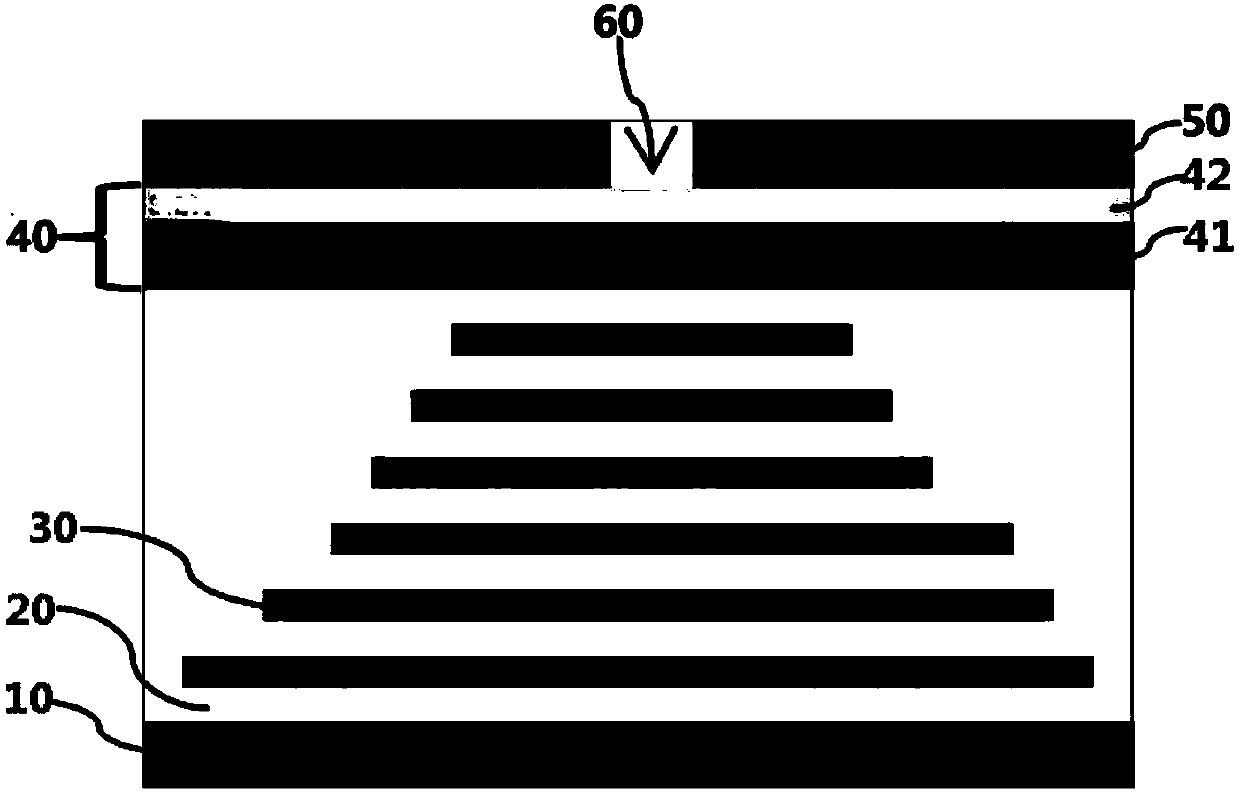
[0039] Exemplary embodiments of the present disclosure will be described in more detail below with reference to the accompanying drawings. Although exemplary embodiments of the present disclosure are shown in the drawings, it should be understood that the present disclosure may be embodied in various forms and should not be limited by the embodiments set forth herein. Rather, these embodiments are provided for more thorough understanding of the present disclosure and to fully convey the scope of the present disclosure to those skilled in the art.

[0040] In the interest of clarity, not all features of an actual implementation are described. In the following description, well-known functions and constructions are not described in detail since they would obscure the invention with unnecessary detail. It should be appreciated that in the development of any actual embodiment, numerous implementation details must be worked out to achieve the developer's specific goals, such as ch...


PUM


Abstract

The invention provides a photoetching-etching technological method of a top select gate cut. A technological step of low temperature oxide (LTO) material deposition is added after photoetching, so that the photoetching critical dimension (PHCD) is reduced equivalently, thereby realizing reduction of the critical dimension of the top select gate cut so as to satisfy the requirement of the miniaturization development of a semiconductor part. Meanwhile, the low temperature oxide (LTO) is used as the deposition material, so that the deposition temperature of the plasma enhanced chemical vapor deposition (PECVD) can be controlled to be about 50 DEG C which is far lower than the bake temperature of 100-120 DEG C of the photo resist material, so that a phenomenon of photo resist material softening in the material deposition can be fully avoided; and by adopting the above-mentioned mode to replace a mode adopting an immersion litho tool, the photoetching critical dimension is reduced economically and stably, thereby further reducing the critical dimension of the top select gate cut.

Description

technical field [0001] The invention relates to the field of semiconductor manufacturing, in particular to a method for manufacturing a 3D NAND flash memory structure, in particular to a photolithography-etching process method for reducing the key dimension of the tangent line of the top-layer selection gate. Background technique [0002] With the development of planar flash memory, the production process of semiconductors has made great progress. However, in recent years, the development of planar flash memory has encountered various challenges: physical limits, existing development technology limits, and storage electron density limits. In this context, in order to solve the difficulties encountered in planar flash memory and to seek lower production costs per unit storage unit, various three-dimensional (3D) flash memory structures have emerged, such as 3D NOR (3D or not) flash memory and 3D NAND (3D NAND) flash memory. [0003] Among them, 3D NAND takes its small size ...

Claims


Application Information

Patent Timeline
Patent Type & Authority Applications(China)
IPC IPC(8): H01L27/11529H01L27/11551H01L27/11573H01L27/11578
CPCH10B41/41H10B41/20H10B43/40H10B43/20
Inventor 何佳刘藩东杨要华王鹏吴林春张若芳夏志良霍宗亮
Owner YANGTZE MEMORY TECH CO LTD
Why Eureka
Try Eureka