Power semiconductor chip and formation method thereof

A technology for power semiconductors and chips, applied in semiconductor devices, semiconductor/solid-state device manufacturing, transistors, etc., can solve problems such as device loss and reliability reduction, and achieve the effects of improving reliability, improving uniformity, and uniform heat distribution

Pending Publication Date: 2018-02-09
嘉兴奥罗拉电子科技有限公司
View PDF0 Cites 1 Cited by
  • Summary
  • Abstract
  • Description
  • Claims
  • Application Information

AI Technical Summary

Problems solved by technology

[0004] However, in some application fields, such as solid-state relays, electronic loads and other devices, it is necessary for power discrete devices to work in the saturation region and maintain their characteristics for a period of time. At this time, a very large loss will occur on the device
The reliability of conventional power devices is drastically reduced at this time

Method used


Image

  • Power semiconductor chip and formation method thereof
  • Power semiconductor chip and formation method thereof
  • Power semiconductor chip and formation method thereof

Examples


Embodiment Construction

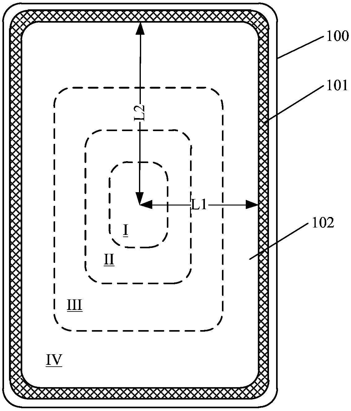
[0026] As mentioned in the background art, when the semiconductor device in the prior art works in a saturated state, a very large loss will be generated on the device, and the reliability will be reduced. The inventors have found that the reduction in reliability of power semiconductor devices is mainly due to the uneven heat distribution inside the device chip in a saturated state, and the temperature at the center of the chip is higher than that at the edge of the chip. This is because the heat generated in the center of the chip is greater than that in the edge area Due to the heat generation, the cells in the central area are easily damaged, and the device loss increases, thereby reducing reliability.

[0027] By reducing the length of the cell channel in the central area of ​​the chip, the present invention realizes the reduction of the calorific value in the central area, so that the internal heating of the chip is uniform, thereby improving the reliability of the power ...


PUM


Abstract

A power semiconductor chip and a method for forming the same, wherein the power semiconductor chip includes: an annular junction terminal region located at the edge of the power semiconductor chip; a cell region surrounded by the junction termination region, and a cell region is formed in the cell region A cell array, the cells are power transistors; the cell area includes more than two sub-areas, one of which is a central sub-area located at the center of the cell area, and the other sub-areas are ring-shaped and surround all of them in turn The central sub-region is set; the length of the cell channel in the same sub-region is the same, and the length of the cell channel in the central sub-region is smaller than the length of the cell channel in other sub-regions. During the working process of the above-mentioned power semiconductor chip, the heat distribution is uniform, and the reliability is higher.

Description

technical field [0001] The invention relates to the technical field of semiconductors, in particular to a power semiconductor chip and a forming method thereof. Background technique [0002] Power semiconductor devices can be divided into uncontrollable devices, half-controlled devices and fully-controlled devices. Among them, uncontrollable devices include various diodes, half-controlled devices include silicon-controlled rectifiers (SCRs), etc., fully-controlled devices include power metal oxide field effect transistors, insulated gate bipolar transistors (IGBTs), bipolar junction type transistor (BJT), etc. [0003] The fully-controlled power device generally works in the switch state, and is in the ohmic region after being turned on, and its voltage drop or on-resistance is extremely low; while it is in the cut-off region after being turned off, with very little leakage, so when used as a switch, the power The loss generated on the device is very small, and the device ...

Claims


Application Information

Patent Timeline
Patent Type & Authority Applications(China)
IPC IPC(8): H01L27/085H01L27/088H01L21/8234
CPCH01L27/085H01L21/823412H01L27/088
Inventor 晋虎万欣李豪高良孙永生杨春益吴善龙
Owner 嘉兴奥罗拉电子科技有限公司
Why Eureka
Try Eureka