Formation method for structure of semi-conductor device

A device structure and semiconductor technology, applied in the fields of semiconductor devices, semiconductor/solid-state device manufacturing, electrical components, etc., can solve the problems of increased complexity of semiconductor devices, inability to effectively reduce device on-resistance, and inability to reduce feature size, etc. Overcome the effects of misalignment

Inactive Publication Date: 2018-02-13
VANGUARD INTERNATIONAL SEMICONDUCTOR CORPORATION
View PDF2 Cites 4 Cited by
  • Summary
  • Abstract
  • Description
  • Claims
  • Application Information

AI Technical Summary

Problems solved by technology

[0003] However, as the functional density of semiconductor devices continues to increase, the complexity of processing and manufacturing semiconductor devices also increases.
For example, due to the limitation of the alignment capability of the conventional lithography exposure equipment, the feature size of the contact structure of the trench gate metal oxide semiconductor field effect transistor cannot be reduced, so the on-resistance of the device cannot be effectively reduced ( onresistance)

Method used


Image

  • Formation method for structure of semi-conductor device
  • Formation method for structure of semi-conductor device
  • Formation method for structure of semi-conductor device

Examples


Embodiment Construction

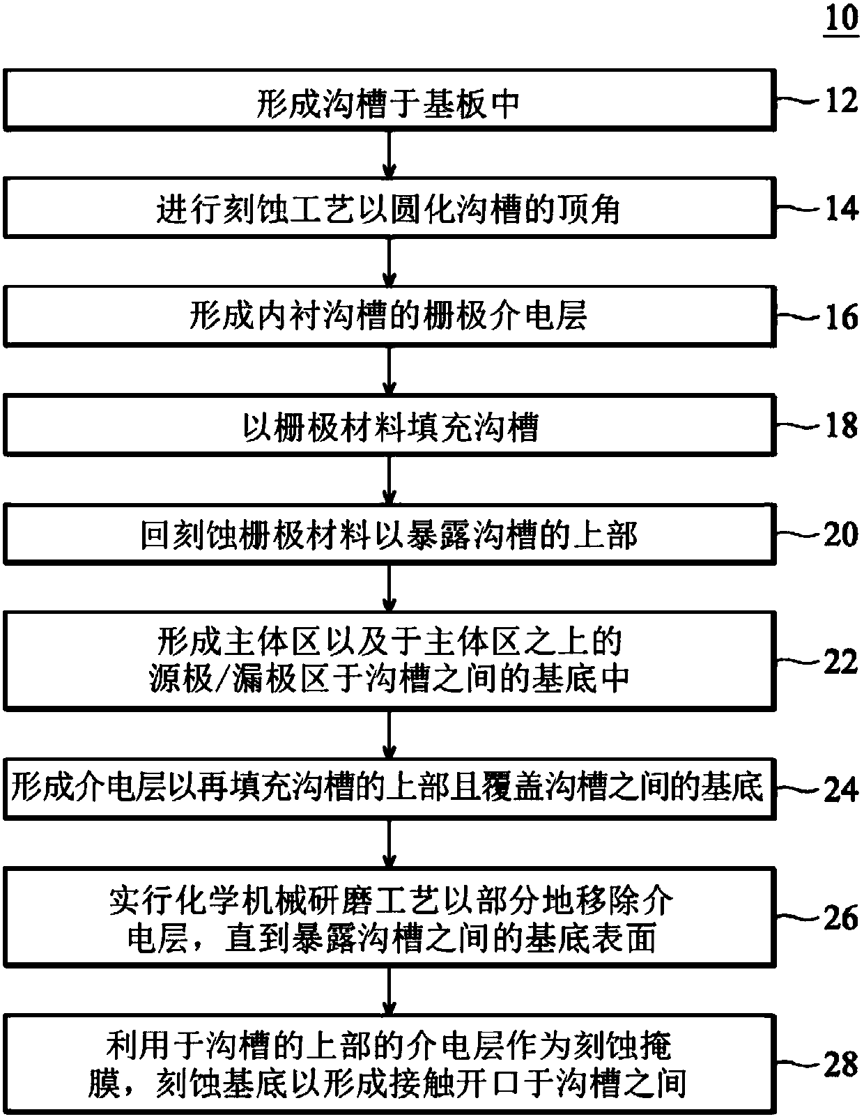
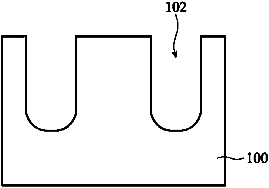
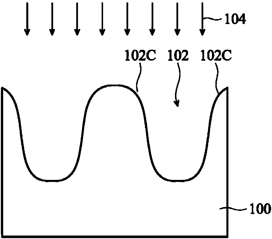
[0044] Many different implementation methods or examples are disclosed below to implement different features of the present invention. Specific elements and examples of their arrangement are described below to illustrate the present invention. Of course, these are only examples and should not limit the scope of the present invention. For example, when the description mentions that a first element is formed on a second element, it may include an embodiment in which the first element is in direct contact with the second element, and may also include an embodiment in which other elements are formed on the first element. An embodiment between and a second element, wherein the first element is not in direct contact with the second element. In addition, repeated symbols or signs may be used in different embodiments, and these repetitions are only for the purpose of simply and clearly describing the present invention, and do not represent a specific relationship between the different...


PUM


Abstract

The invention provides a formation method for structure of semi-conductor device, which includes forming several grooves in the base; forming a gate dielectric layer in the grove as an inner liner; filling the grooves with gate materials; re-etching the gate materials to make the top of the grooves be exposed; filling the top of grooves with a first dielectric layer which also covers the surface of the base between two grooves; implementing a first chemical and mechanical grinding techniques to partly eliminate the first dielectric layer, until the surface of the base between two grooves is exposed; using the first dielectric layer, which is used to form the top of the grooves, as an etching mask; and etching the base to form self-aligned contact openings between the grooves by exposing the surface of the base to the air.

Description

technical field [0001] The present invention relates to a method for forming a semiconductor device structure, and in particular to a method for forming a trench gate metal-oxide-semiconductor field effect transistor (trench gate MOSFET). Background technique [0002] The semiconductor industry continues to improve the integration density of different electronic components. By continuously reducing the minimum component size, more components can be integrated in a given area. For example, the trench gate metal-oxide-semiconductor field effect transistor, which is widely used in power switch devices, utilizes a vertical structure design to increase functional density. It utilizes the backside of the chip as the drain, and manufactures the sources and gates of multiple transistors on the front side of the chip. [0003] However, as the functional density of semiconductor devices continues to increase, the complexity of processing and manufacturing semiconductor devices also i...

Claims


Application Information

Patent Timeline
Patent Type & Authority Applications(China)
IPC IPC(8): H01L21/336H01L21/28
Inventor 李宗晔林治平
Owner VANGUARD INTERNATIONAL SEMICONDUCTOR CORPORATION
Why Eureka
Try Eureka