Printed circuit board with reliability-improved embedded resistor and manufacturing method thereof
A technology for printed circuit boards and manufacturing methods, which is applied in the manufacture of printed circuits, removal of conductive materials by chemical/electrolytic methods, printed circuits, etc., can solve the problems of resistance layer damage, low resistivity, resistance changes, etc. The effect of electrical performance
- Summary
- Abstract
- Description
- Claims
- Application Information
AI Technical Summary
Problems solved by technology
Method used
Image

Examples
Embodiment 1
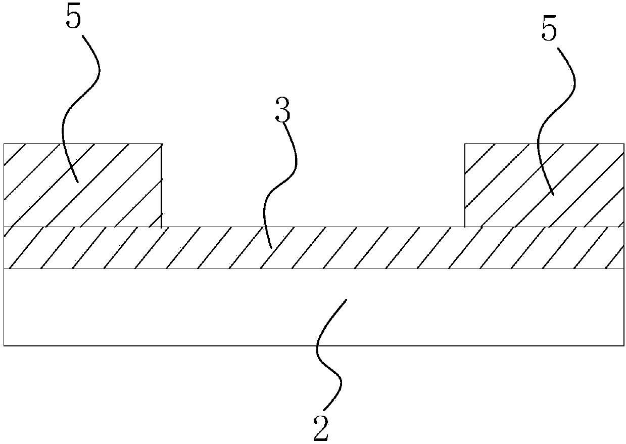
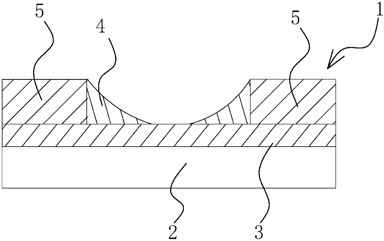
[0032] Such as image 3 As shown, the printed circuit board that improves the reliability of the embedded resistance includes a circuit board body 1, and the circuit board body 1 includes an insulating dielectric layer 2, a resistance layer 3, a resistance protection layer 4 and at least two conductor layers 5, where The resistance layer 3 is directly covered on the upper surface of the insulating medium layer 2, the conductor layer 5 is distributed and arranged on the upper surface of the resistance layer 3 in turn, and the resistance protection layer 4 is located at the junction of the resistance layer 3 and the conductor layer 5.
[0033] Further, the cross section of the resistance protection layer 4 is a right-angled triangle structure whose hypotenuse is a concave curve, and in order to ensure strength, the top of the resistance protection layer 4 is flush with the upper surface of the conductor layer 5 or the upper surface of the resistance layer 3 .
[0034] Wherein, ...
Embodiment 2
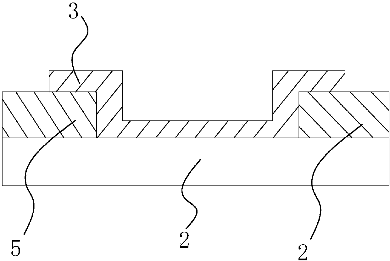
[0040] Such as Figure 4 As shown, the structure, principle and implementation steps of this embodiment are similar to those of Embodiment 1, the difference is that the conductor layer 5 here is directly and successively distributed on the upper surface of the insulating medium layer 2, and the resistance layer 3 is covered on the conductor layer. 5, and the middle part of the resistance layer 3 has a bent part bent downward, and the resistance protection part is located on both sides of the upper end of the bent part.
[0041] The method of this embodiment includes the following steps: 1. Making an inner layer plate, including preparing an insulating medium layer 2 and laminating a conductor layer 5 that does not contain a resistance layer 3 on the upper surface of the insulating medium layer 2; 2. Making a conductor circuit, including Paste the first photoresist layer on the conductive layer body, perform the first exposure, the first development, the first etching, and the ...
PUM
 Abstract
Description
Claims
Application Information
 - R&D
- Intellectual Property
- Life Sciences
- Materials
- Tech Scout
- Unparalleled Data Quality
- Higher Quality Content
- 60% Fewer Hallucinations
Browse by: Latest US Patents, China's latest patents, Technical Efficacy Thesaurus, Application Domain, Technology Topic, Popular Technical Reports.
© 2025 PatSnap. All rights reserved.Legal|Privacy policy|Modern Slavery Act Transparency Statement|Sitemap|About US| Contact US: help@patsnap.com