Method and device for extracting parasitic inductances of IGBT modules

A technology of parasitic inductance and extraction method, which is applied in electrical digital data processing, CAD circuit design, special data processing applications, etc., can solve the problems of IGBT module stray parameter evaluation and stray parameter extraction, etc., to avoid inconvenience and accurate. The effect of data reference

Inactive Publication Date: 2018-03-06
GLOBAL ENERGY INTERCONNECTION RES INST CO LTD
View PDF6 Cites 7 Cited by
  • Summary
  • Abstract
  • Description
  • Claims
  • Application Information

AI Technical Summary

Problems solved by technology

The existing experimental measurement method establishes an inductance-capacitance (LC) model of lumped parameters, that is, all parasitic inductance and parasitic capacitance parameters in the IGBT module are set as a total number in a centralized manner. The stray parameters of each branch of the complex IGBT module are extracted in detail, so it is impossible to make accurate and effective stray parameter evaluation for the IGBT module in the early stage of circuit design

Method used


Image

  • Method and device for extracting parasitic inductances of IGBT modules
  • Method and device for extracting parasitic inductances of IGBT modules
  • Method and device for extracting parasitic inductances of IGBT modules

Examples


Embodiment 1

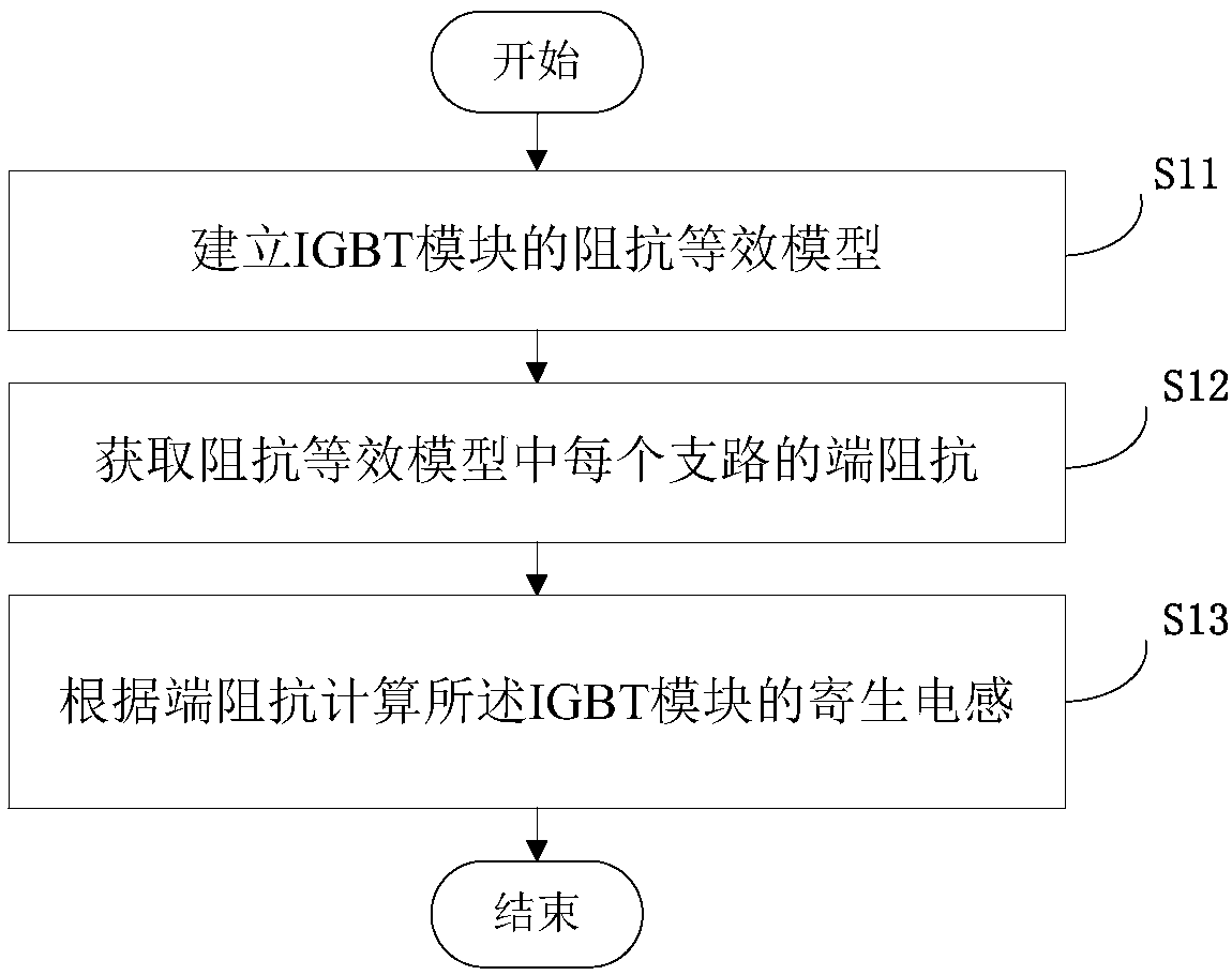
[0027] This embodiment provides a method for extracting the parasitic inductance of the IGBT module, which is suitable for extracting the parasitic inductance of the IGBT module, such as figure 1 As shown, the method includes the following steps:

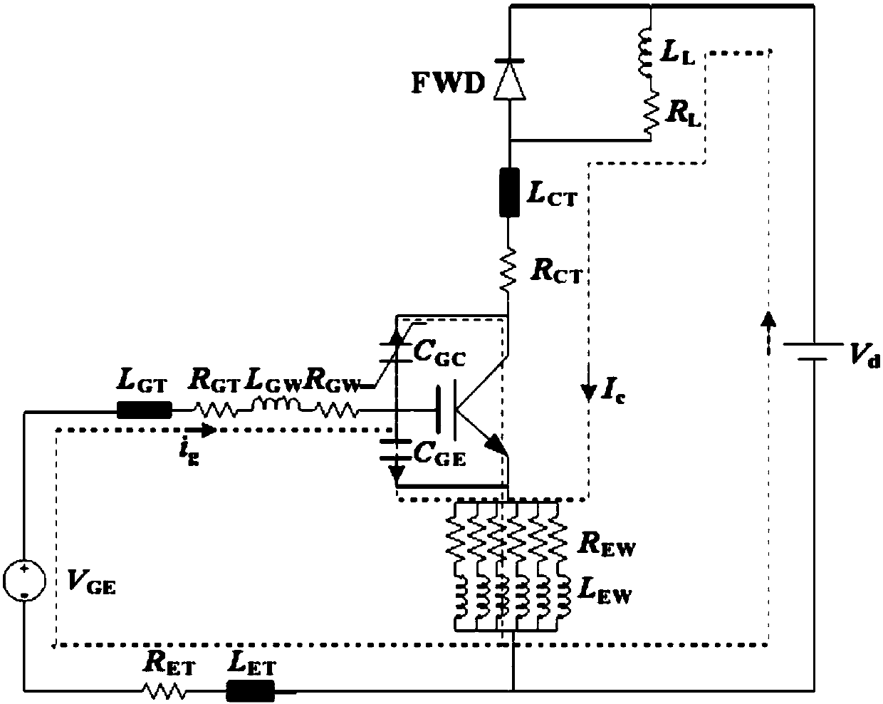
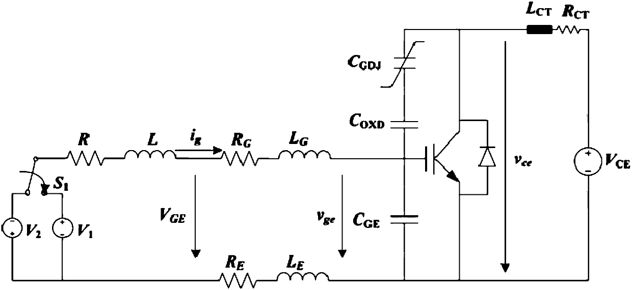
[0028] S11: Establish the impedance equivalent model of the IGBT module; that is, establish the corresponding impedance equivalent model according to the characteristics of each circuit inside the IGBT module. A suitable impedance equivalent model can help to extract the parasitic inductance more accurately, so in the model established At this time, the internal circuit structure of different IGBT modules should be fully considered, and the most suitable impedance equivalent model has been established.

[0029] As a specific implementation, step S11 may specifically include: obtaining the equivalent gate circuit of the IGBT chip in the IGBT module; obtaining the three-terminal impedance network of the IGBT module according to the eq...

Embodiment 2

[0051] This embodiment provides a parasitic inductance extraction device for an IGBT module, such as Figure 5 As shown, the device includes: an establishment module 51, an acquisition module 52 and a calculation module 53, and the main functions of each module are as follows:

[0052] The establishment module 51 is configured to establish an impedance equivalent model of the IGBT module; for details, refer to the detailed description of step S11 in Embodiment 1.

[0053] The acquiring module 52 is configured to acquire the terminal impedance of each branch in the impedance equivalent model; refer to the detailed description of step S12 in Embodiment 1 for details.

[0054] The calculating module 53 is used for calculating the parasitic inductance of the IGBT module according to the terminal impedance. For details, refer to the detailed description of step S13 in Embodiment 1.

[0055] As a preferred solution, establishing the impedance equivalent model of the IGBT module in...


PUM


Abstract

The invention provides a method and device for extracting parasitic inductances of IGBT modules. The method comprises the following steps of: establishing an impedance equivalent model of an IGBT module; obtaining an end impedance of each branch in the impedance equivalent module; and calculating a parasitic inductance of the IGBT module according to the end impedances. According to the method anddevice, the impedance equivalent model corresponding to the IGBT module is established according to characteristics of each circuit in the IGBT module, the end impedance of each branch in the impedance equivalent module is obtained through an experiment measurement manner, the parasitic inductance of each branch is calculated according to the end impedance of each branch and internal inductance distribution condition of the IGBT module, and finally the parasitic inductance of the whole IGBT module is obtained. Compared with the prior art, the method and device have the advantage that the extraction of parasitic inductance parameters is separately divided so that the inconvenience of data analysis due to setting the parasitic parameters into lumped parameters is avoided and more correct data reference is provided for the packaging design of the IGBT module.

Description

technical field [0001] The invention relates to the technical field of electronic devices, in particular to a method and device for extracting parasitic inductance of an IGBT module. Background technique [0002] In recent years, with the advancement of power electronic device manufacturing technology and the improvement of current conversion technology, the application field of power conversion devices based on insulated gate bipolar transistor (Insulated gate bipolar transistor, IGBT) devices has been greatly expanded. With the optimization of device structure and the emergence of new technology, the operating frequency of IGBT has reached tens or even nearly hundreds of kHz, and the switching time has been reduced to the microsecond level, and even reached the nanosecond level at low power. The trend of high frequency makes the power density of the power converter increase, the dynamic response ability is improved, and the audio noise is reduced. However, in the actual c...

Claims


Application Information

Patent Timeline
Patent Type & Authority Applications(China)
IPC IPC(8): G06F17/50
CPCG06F30/367G06F30/39
Inventor 张喆李现兵张朋林仲康石浩韩荣刚田丽纷武伟
Owner GLOBAL ENERGY INTERCONNECTION RES INST CO LTD
Why Eureka
Try Eureka