Vertical double-diffusion metal oxide semiconductor device and manufacturing method thereof

An oxide semiconductor and vertical double-diffusion technology, which is applied in semiconductor/solid-state device manufacturing, semiconductor devices, electrical components, etc., can solve problems such as large reverse transmission capacitance, large gate coverage area, and reduced device withstand voltage, achieving Effects of reducing reverse capacitance, shortening switching time, and reducing reverse recovery time

Inactive Publication Date: 2018-03-09
WUXI CHINA RESOURCES HUAJING MICROELECTRONICS
View PDF2 Cites 5 Cited by
  • Summary
  • Abstract
  • Description
  • Claims
  • Application Information

AI Technical Summary

Problems solved by technology

[0004] Due to the large gate coverage area of ​​conventional VDMOS devices, the reverse transmission capacitance is large, and the switching power consumption is large
At present, the common method to reduce the reverse transfer capacitance is to use a split gate structure, which is to etch away part of the silicon gate in the middle of the N-doped region on the conventional structure. The reverse transfer capacitance is much lower than the conventional structure, but due to the etching away The silicon gate on the surface will reduce the withstand voltage of the device

Method used


Image

  • Vertical double-diffusion metal oxide semiconductor device and manufacturing method thereof
  • Vertical double-diffusion metal oxide semiconductor device and manufacturing method thereof
  • Vertical double-diffusion metal oxide semiconductor device and manufacturing method thereof

Examples


Embodiment 1

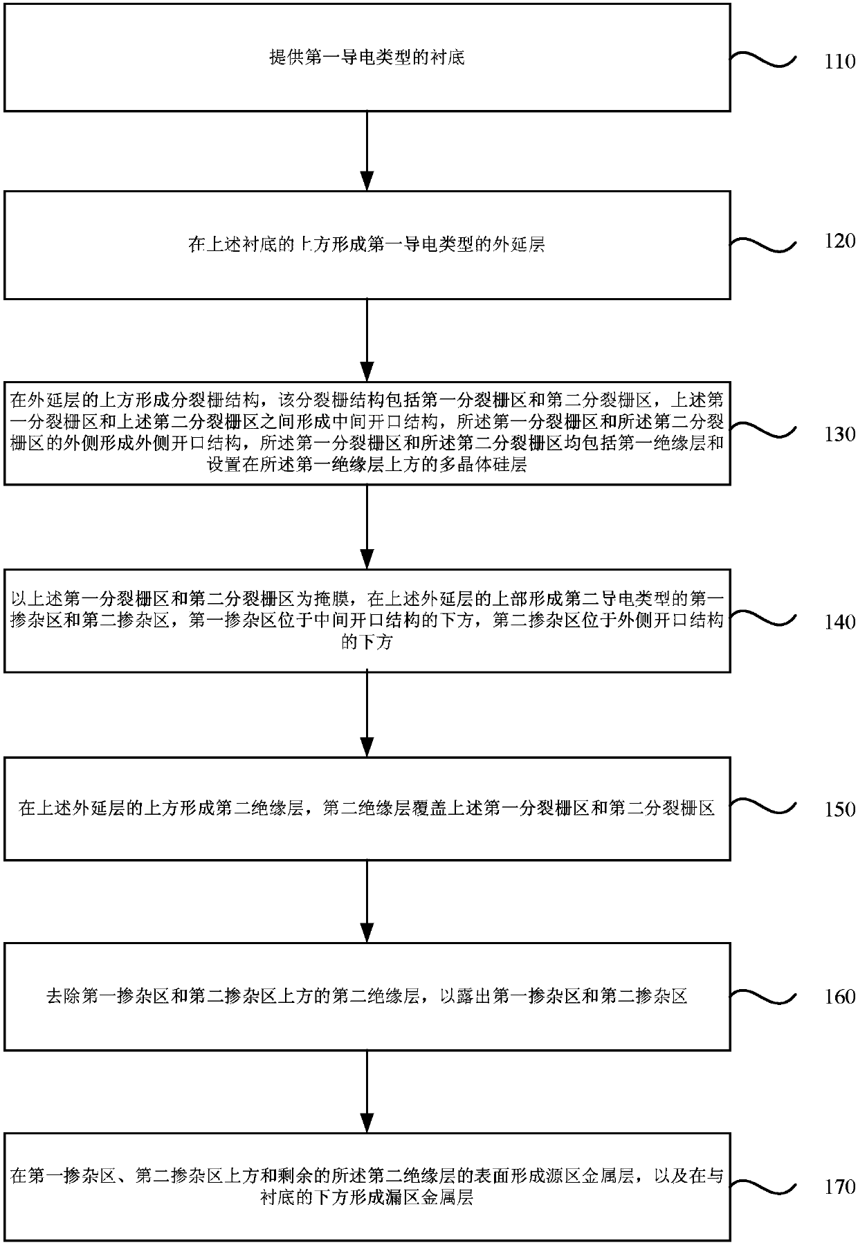
[0037] figure 1 It is a schematic flowchart of a method for fabricating a vertical double-diffused metal oxide semiconductor device provided in Embodiment 1 of the present invention. Figure 2a - FIG. 2m is a cross-sectional view corresponding to each step of a method for fabricating a vertical double-diffused metal oxide semiconductor device according to Embodiment 1 of the present invention.

[0038] see figure 1 , the present embodiment provides a method for fabricating a vertical double-diffused metal oxide semiconductor device, the method comprising the following steps:

[0039] Step 110, providing a substrate of the first conductivity type.

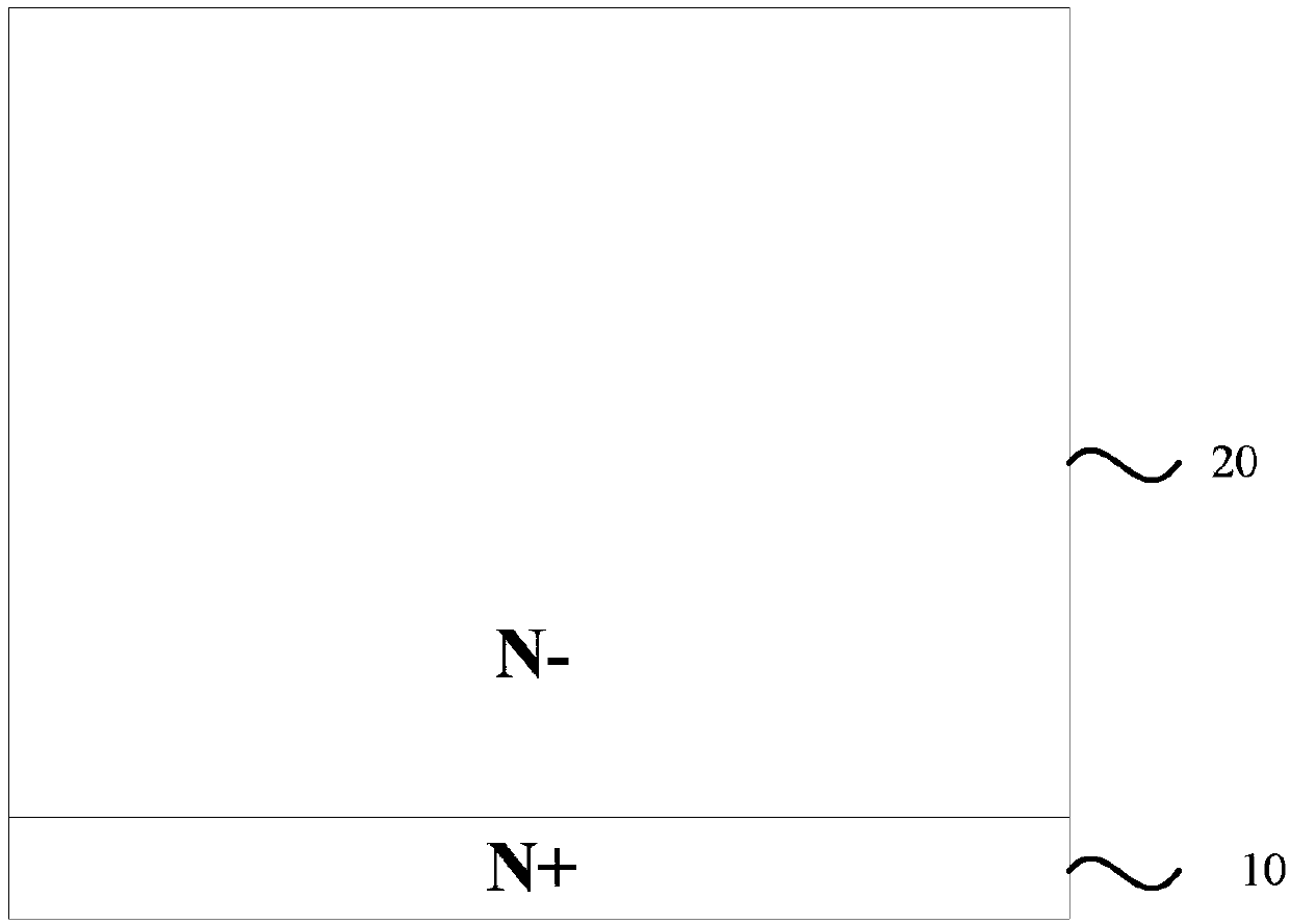
[0040] Referring to 2a, this embodiment takes an N-channel VDMOS device as an example, where the first conductivity type is N-type, and this embodiment needs to provide an N-type substrate. In this embodiment, the single crystal silicon wafer is heavily doped with N-type ions, which can be represented by N+, and the N-type ions c...

Embodiment 2

[0068] Embodiment 2 of the present invention provides a vertical double-diffused metal oxide semiconductor device, which can be manufactured by the preparation method of Embodiment 1. Specifically, the vertical double-diffused metal oxide semiconductor device provided by the embodiment of the present invention includes :

[0069] A substrate of the first conductivity type.

[0070] The epitaxial layer of the first conductivity type is located above the substrate.

[0071] The split gate structure, located above the epitaxial layer, includes a first split gate region and a second split gate region, an intermediate opening structure is formed between the first split gate region and the second split gate region, and the first split gate region and the second split gate region The outer side of the split gate region is an outer opening structure, and both the first split gate region and the second split gate region include a first insulating layer and a polysilicon layer disposed...


PUM


Abstract

The embodiments of the invention provide a vertical double-diffusion metal oxide semiconductor device and a manufacturing method thereof. The method comprises the steps of: providing a substrate of afirst conductive type; forming an epitaxial layer of the first conductive type on the substrate; forming a split gate structure on the epitaxial layer, a first split gate region and a second split gate region each comprising a first insulating layer and a polycrystalline silicon layer on the first insulating layer; forming a first doped region and a second doped region of a second conductive typeon the upper surface of the epitaxial layer; forming a second insulating layer on the epitaxial layer, the second insulating layer covering the first split gate region and the second split gate region; and removing the second insulating layer on the first doped region and the second doped region to expose the first doped region and the second doped region. The embodiments of the invention providea manufacturing method and a structure of a vertical double-diffusion metal oxide semiconductor device, which can reduce the reverse capacitance and the switching time of the device and improve the voltage endurance of the device.

Description

technical field [0001] The invention relates to the technical field of semiconductor manufacturing, in particular to a vertical double-diffused metal oxide semiconductor device and a preparation method thereof. Background technique [0002] Power semiconductor devices are essential core devices for realizing power conversion and control. With the establishment and promotion of the concept of energy saving, emission reduction and green environmental protection, the importance of power semiconductors is increasing day by day, and the application prospects are getting wider and wider. The country has made it an important strategic goal to promote the industrial development of new power electronic chips and devices. [0003] Vertical double-diffused metal oxide semiconductor (VDMOS) devices have the advantages of high input impedance, low driving power, fast switching speed, and good thermal stability, and have become the most widely used new power devices. Using VDMOS as a sw...

Claims


Application Information

Patent Timeline
Patent Type & Authority Applications(China)
IPC IPC(8): H01L29/78H01L21/336
CPCH01L29/7802H01L29/66712
Inventor 张新李巍王荣华
Owner WUXI CHINA RESOURCES HUAJING MICROELECTRONICS
Why Eureka
Try Eureka