Photoelectric detecting structure and preparation method thereof

A photodetection, photodiode technology, applied in circuits, electrical components, electrical solid devices, etc., can solve the problems of low photoresponsivity, the influence of visible light divergent image quality, etc., to achieve high photoresponsivity, good image clarity, reduce light the divergent effect of

Inactive Publication Date: 2018-03-13
SHANGHAI IRAY TECH
View PDF4 Cites 14 Cited by
  • Summary
  • Abstract
  • Description
  • Claims
  • Application Information

AI Technical Summary

Problems solved by technology

[0006] In view of the shortcomings of the prior art described above, the purpose of the present invention is to provide a photoelectric detection structure and its preparation method, which are used to solve the problem of divergence of visible light, crosstalk affecting image quality, and low photoresponsivity in the prior art. question

Method used


Image

  • Photoelectric detecting structure and preparation method thereof
  • Photoelectric detecting structure and preparation method thereof
  • Photoelectric detecting structure and preparation method thereof

Examples


Embodiment 1

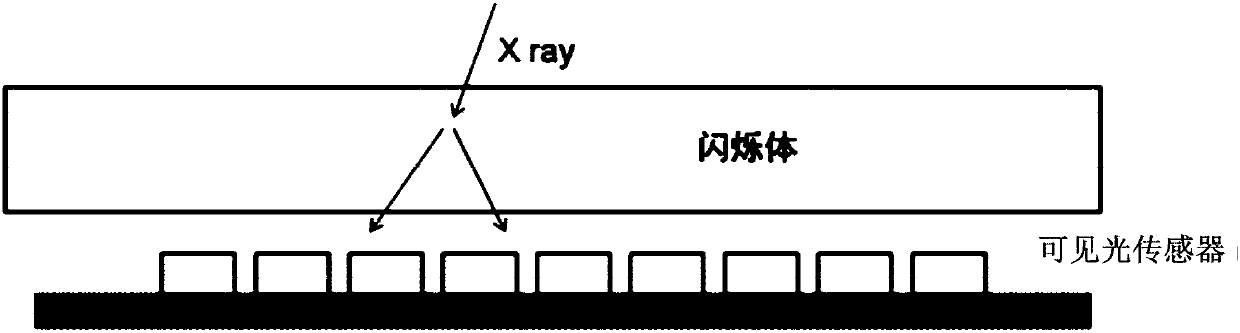
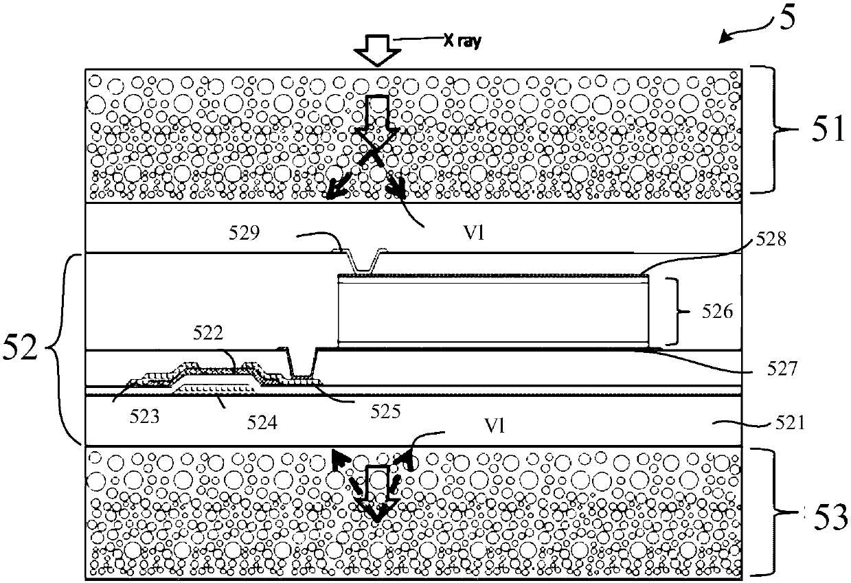
[0047] Such as image 3 As shown, the present invention provides a kind of photodetection structure 5, and described photodetection structure 5 comprises at least:

[0048] The first scintillator layer 51 , the first visible light sensor 52 , and the second scintillator layer 53 .

[0049] Such as image 3 As shown, the first scintillator layer 51 is located on the X-ray (X ray) receiving surface of the photodetection structure 5, and is used to absorb X-rays with lower energy and convert X-rays into visible light V1, and visible light V1 is obtained from The output from the first scintillator layer 51 is detected by the first visible light sensor 52 .

[0050] Specifically, the material of the first scintillator layer 51 includes but not limited to cesium iodide or gadolinium oxysulfide, and any material that can convert X-rays into visible light is suitable for the present invention, not limited to this embodiment.

[0051] Such as image 3 As shown, the second scintilla...

Embodiment 2

[0060] This embodiment provides a photoelectric detection structure, which is basically the same as that of Embodiment 1, except that the substrate 521 is a fiber optical plate.

[0061] Specifically, such as Figure 4 As shown, the fiber guide plate is provided with a plurality of fiber guides perpendicular to the surface, and the visible light generated by the second scintillator layer 53 is refracted to the first visible light sensor 52 through each fiber guide and absorbed, which can effectively Reduce the divergence of visible light.

Embodiment 3

[0063] This embodiment provides a photodetection structure, which is basically the same as that of Embodiment 1 and Embodiment 2, except that the lower layer of the second scintillator layer 53 also includes a second visible light sensor (not shown in the figure). , used to convert the visible light passing through the second scintillator layer 53 into charges and store them in the second visible light sensor.

[0064] Further, it can also be extended to an interphase distribution structure of multi-layer scintillator layers and multi-layer visible light sensors. The more layers, the shorter the path of visible light, the slighter the divergence of light, and the clearer the image; at the same time, the scintillator layers of different layers use independent visible light sensors, the greater the X-ray energy, the deeper the irradiation depth, thus achieving Detection of multi-level X-rays.


PUM


Abstract

The invention provides a photoelectric detecting structure and a preparation method thereof. The photoelectric detecting structure comprises the components of a first scintillator layer which is usedfor absorbing X ray with relatively low energy and converting the X ray to visible light; a second scintillator layer which is used for absorbing the X ray with relatively high energy and converting the X ray to the visible light; and a first visible light sensor which is arranged between the first scintillator layer and the second scintillator layer and is used for converting the visible light that penetrates through the first scintillator layer and the visible light that is reflected by the second scintillator layer to electric charges and storing electric charges into the first visible light sensor. A substrate is supplied. The first visible light sensor is formed on the substrate through a semiconductor process in a layer-by-layer manner. The first scintillator layer is formed on the first surface of the first visible light sensor, and then the second scintillator layer is formed on the second surface of the first visible light sensor. The photoelectric detecting structure and thepreparation method have advantages of relatively high image definition on the condition of high-energy ray and higher photoresponsivity.

Description

technical field [0001] The invention relates to the field of medical image diagnosis, in particular to a photoelectric detection structure and a preparation method thereof. Background technique [0002] Flat-panel image sensors are usually used in medical radiation imaging, industrial flaw detection, security inspection and other fields. Flat-panel image sensors, especially large-size image sensors, usually have an area of ​​tens of centimeters and millions to tens of millions of pixels. In the application of X-ray image detectors, the area generally requires an area of ​​43cm*43cm, so currently amorphous Silicon technology (monocrystalline silicon is currently generally 24 to 30 cm in diameter). [0003] Such as figure 1 As shown, currently used amorphous silicon flat panel detectors usually have a multi-layer stacked structure. Including, the upper scintillator, which converts the incident X-rays into visible light. Visible light is irradiated onto a visible light sens...

Claims


Application Information

Patent Timeline
Patent Type & Authority Applications(China)
IPC IPC(8): H01L27/14H01L27/146H01L31/115H01L31/18
CPCH01L27/146H01L27/14601H01L27/14683H01L31/115H01L31/18Y02P70/50
Inventor 金利波
Owner SHANGHAI IRAY TECH
Why Eureka
Try Eureka