
Double-sided-folded gate-controlled source/drain double tunneling type bidirectional conductive transistor and manufacturing method thereof
A bidirectional conduction, source-drain technology, applied in semiconductor/solid-state device manufacturing, semiconductor devices, electrical components, etc., can solve the problems that transistors can only be used as one-way switches and sub-threshold swings cannot be reduced, and achieve excellent gate electrodes Control ability, effect of low subthreshold swing
- Summary
- Abstract
- Description
- Claims
- Application Information
AI Technical Summary
Problems solved by technology
Method used
Image

Examples
Embodiment Construction
[0096] Below in conjunction with accompanying drawing, the present invention will be further described:
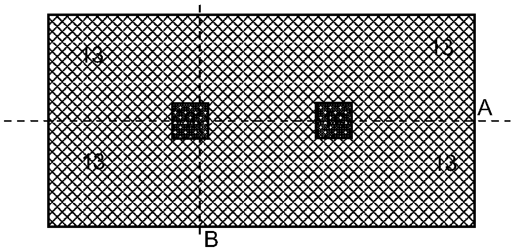
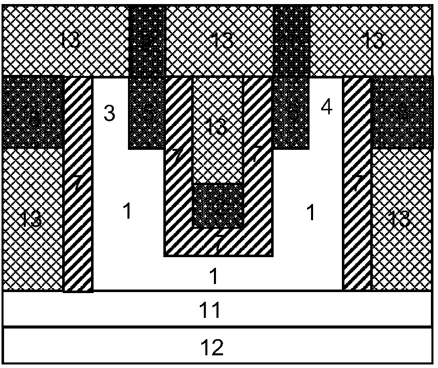
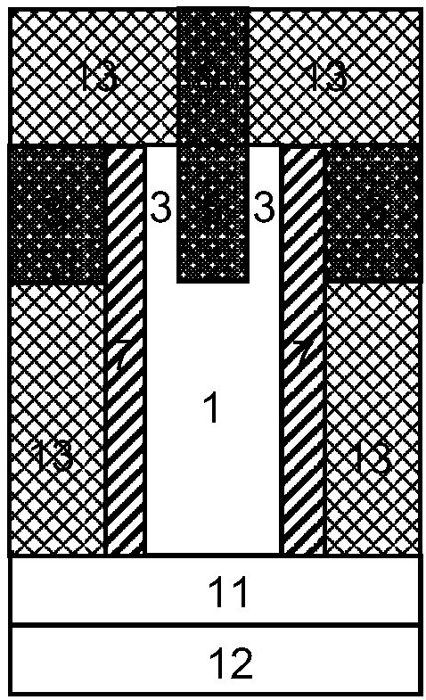
[0097] Such as figure 1 , figure 2 and image 3 As shown, a double-side folded gate-controlled source-drain double-tunneling bidirectional conduction transistor includes a silicon substrate 12 of an SOI wafer, and a substrate insulating layer 11 of the SOI wafer is above the silicon substrate 12 of the SOI wafer. , above the substrate insulating layer 11 of the SOI wafer is a single crystal silicon film 1, a barrier adjustment gate 2, a partial area of the gate electrode insulating layer 7 and a partial area of the insulating dielectric barrier layer 13; wherein, the single crystal silicon thin film 1 For impurity concentration below 10 16 cm -3 The monocrystalline silicon semiconductor material has a U-shaped groove structure; the heavily doped source-drain interchangeable region a5 and the heavily doped source-drain interchangeable region b6 perform ion implanta...
PUM
 Abstract
Description
Claims
Application Information