A method for optimizing the return loss of bga solder joints
A return loss and solder joint technology, applied in the field of signal integrity of microelectronic packaging, can solve problems such as system performance degradation, data loss, and misjudgment of signal integrity
- Summary
- Abstract
- Description
- Claims
- Application Information
AI Technical Summary
Problems solved by technology
Method used
Image
Examples
Embodiment
[0041] refer to Figure 6 , a method for optimizing the return loss of a BGA solder joint, comprising the steps of:
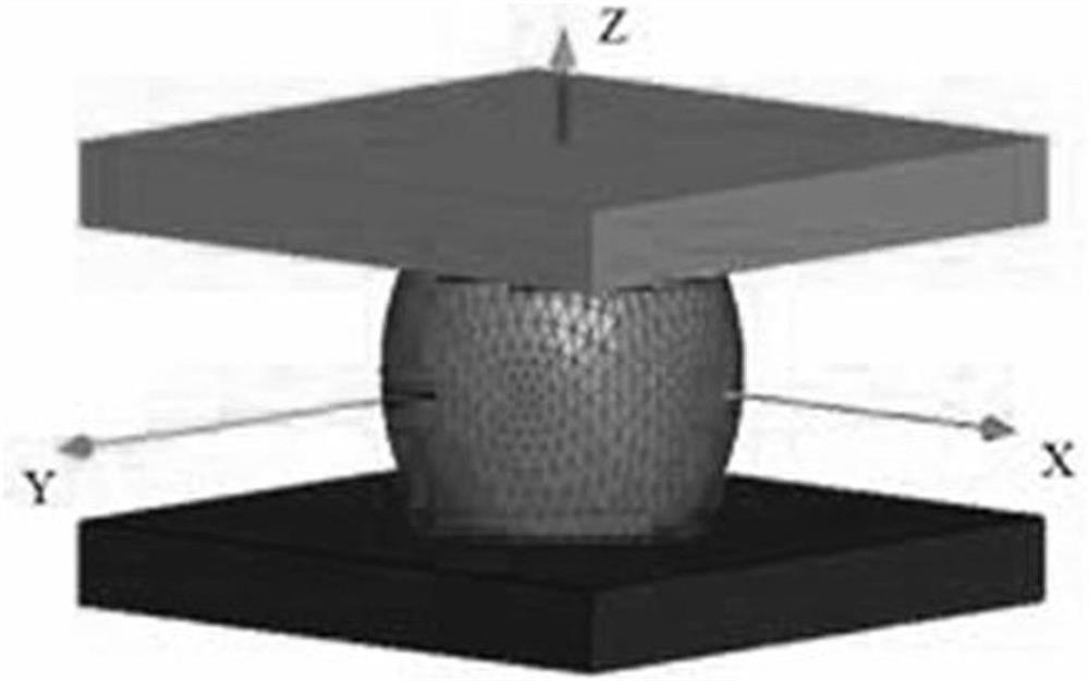
[0042] 1) Establish a BGA solder joint signal integrity analysis model: the model is a sequentially stacked printed circuit board, solder joint and organic substrate from bottom to top;
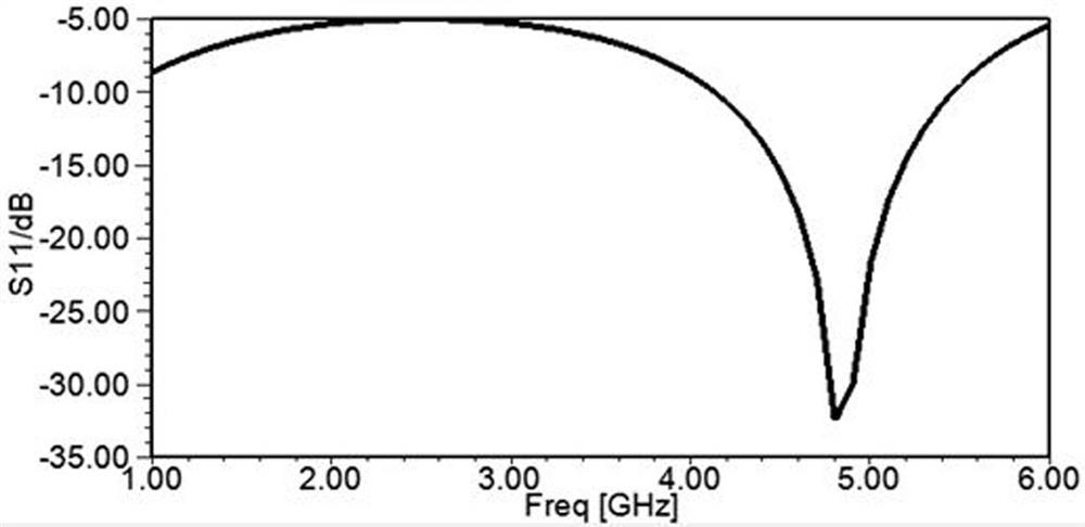
[0043] 2) Obtain the return loss of the BGA solder joint: apply wave port excitation to the model built in step 1), then use HFSS software to simulate and analyze the model to obtain the return loss of the BGA solder joint;
[0044] 3) Establish the influencing factors of the signal integrity of the BGA solder joint: the influencing factors are the maximum radial size of the solder joint, the height of the solder joint, and the diameter of the pad;
[0045] 4) Establish the parameter level values of the factors affecting the signal integrity of BGA solder joints: select three sets of horizontal values of the maximum radial size of the solder joints, the height of the sold...
PUM
 Abstract
Description
Claims
Application Information


