LED packaging method
An LED packaging and ultraviolet technology, which is applied to semiconductor devices, electrical components, circuits, etc., can solve the problems of insufficient concentration of light source lighting, reduced light intensity, and reduced LED service life, so as to suppress the total reflection effect and solve the problem of light transmittance. The effect of reducing and increasing the cooling effect
- Summary
- Abstract
- Description
- Claims
- Application Information
AI Technical Summary
Problems solved by technology
Method used
Image
Examples
Embodiment 1
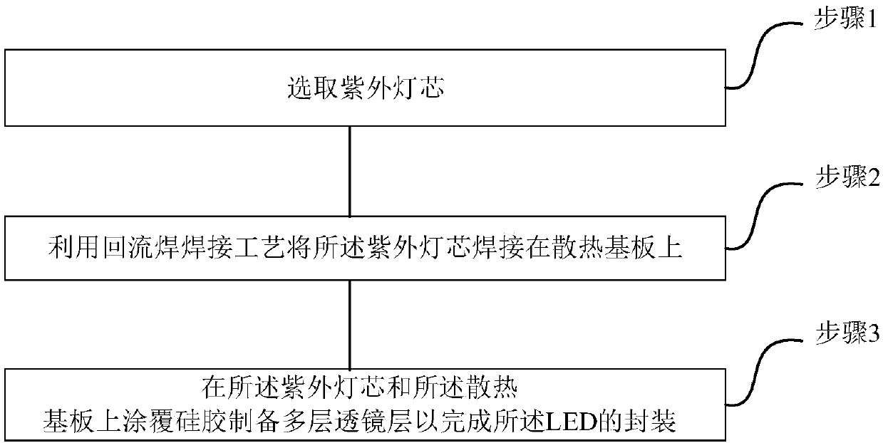
[0069] See figure 1 , figure 1 It is a flow chart of an LED packaging method provided by an embodiment of the present invention. The method comprises the steps of:
[0070] Step 1. Select the UV wick;
[0071] Step 2, using a reflow soldering process to weld the ultraviolet wick on the substrate;
[0072] Step 3, coating silica gel on the ultraviolet wick and the substrate to prepare a multi-layer lens layer to complete the packaging of the LED.
[0073] Further, the outside of the substrate in step 2 is provided with circular grooves along the width direction and parallel to the plane of the substrate; wherein, the diameter of the circular grooves is 0.3-2 mm, and the distance between the circular grooves is 0.5-10 mm .
[0074] Among them, for step 2, may include:
[0075] printing solder onto the UV wick;
[0076] Carrying out the crystal-bonding inspection of the ultraviolet wick printed with solder;
[0077] The ultraviolet wick printed with solder is soldered to ...
Embodiment 2
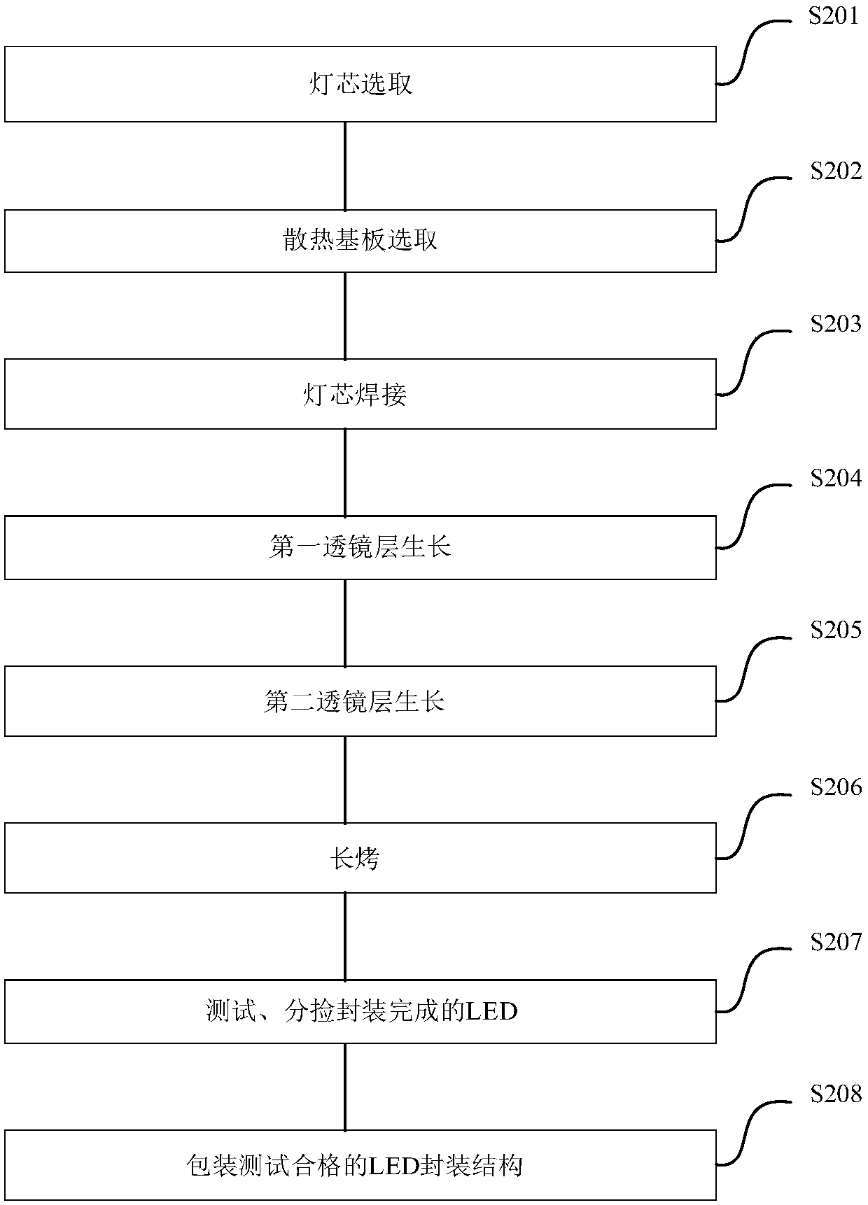
[0119] See figure 2 , figure 2 It is a flowchart of a double-layer lens layer LED packaging method provided by an embodiment of the present invention. On the basis of the above embodiments, this embodiment will introduce in detail the process flow of the double-layer lens layer LED package proposed by the present invention. The method includes:
[0120] S201. Wick selection
[0121] Select the ultraviolet wick as the wick of the LED.
[0122] S202, substrate selection
[0123] Only a part of the energy in the LED input power is converted into light energy, and the rest is converted into heat energy. Therefore, for LED chips, especially LED chips with high power density, how to control their thermal energy is an important issue that LED manufacturing and lamps should focus on solving. The heat of high-power diodes, high-power triodes, IGBTs, and MOSFETs can be dissipated through an external radiator with almost unlimited size installed on the instrument case, or a cooli...
Embodiment 3
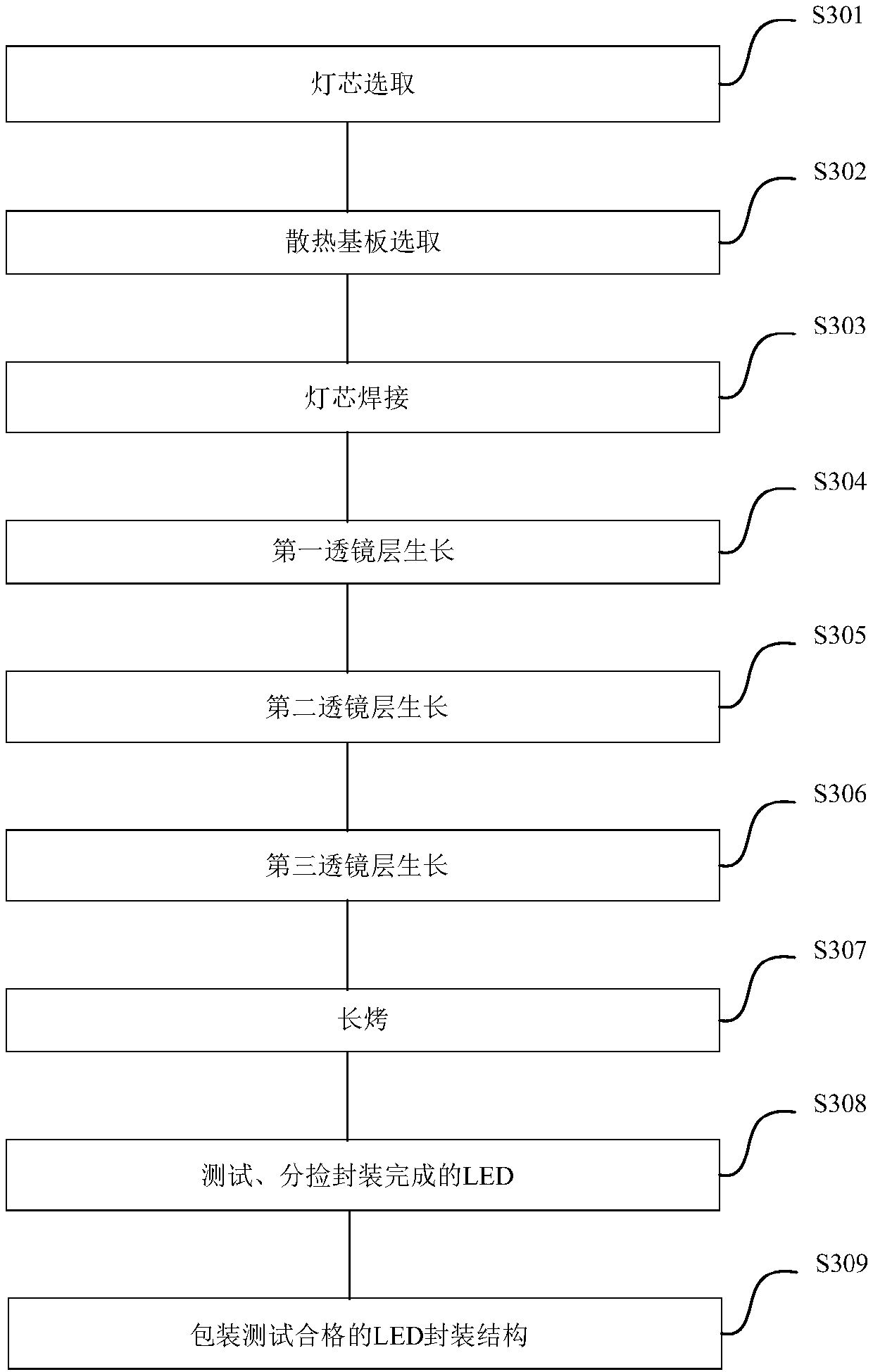
[0167] See image 3 , image 3 It is a flow chart of a three-layer lens layer LED packaging method provided by an embodiment of the present invention. On the basis of the above embodiments, this embodiment will introduce in detail the process flow of the three-layer lens layer LED package proposed by the present invention. include:
[0168] S301. Wick selection
[0169] Select the ultraviolet wick as the wick of the LED.
[0170] S302. Substrate selection
[0171] S3021. Preparation of support / substrate
[0172] Metal copper is selected as the material of the substrate, and the thickness of the substrate is 0.5-10 mm. The outer side of the substrate has circular grooves along the width direction and parallel to the plane of the substrate; wherein, the diameter of the circular grooves is 0.3-2mm, and the distance between the circular grooves is 0.5-10mm. The round groove can be formed by direct casting, or directly drilled on the copper substrate along the width directio...
PUM
 Abstract
Description
Claims
Application Information


