Voltage peak absorption circuit

A technology of absorbing circuit and voltage spike, which is applied in the field of switching power supply, can solve problems such as complex structure, power supply reliability threat, product reliability, volume, and efficiency impact, and achieve the effects of reducing volume, improving electromagnetic compatibility, and simplifying structure

Active Publication Date: 2018-03-23
天津航空机电有限公司
View PDF5 Cites 7 Cited by
  • Summary
  • Abstract
  • Description
  • Claims
  • Application Information

AI Technical Summary

Problems solved by technology

This not only means that designers must choose expensive high-voltage power switch tubes, but also poses a potential threat to the reliability of the power supply. Therefore, it is necessary to set up various snubber absorption circuits to suppress it.
[0003] At present, there are many kinds of voltage spike absorbing circuits that can achieve the purpose of buffering and absorbing, but the current designed voltage spike absorbing circuits often require multiple controls and more magnetic components, the structure is complex, and the reliability, size, and efficiency of the product are all there. influences

Method used


Image

  • Voltage peak absorption circuit
  • Voltage peak absorption circuit
  • Voltage peak absorption circuit

Examples


Embodiment 1

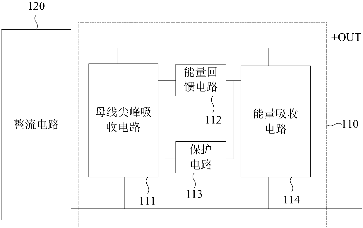
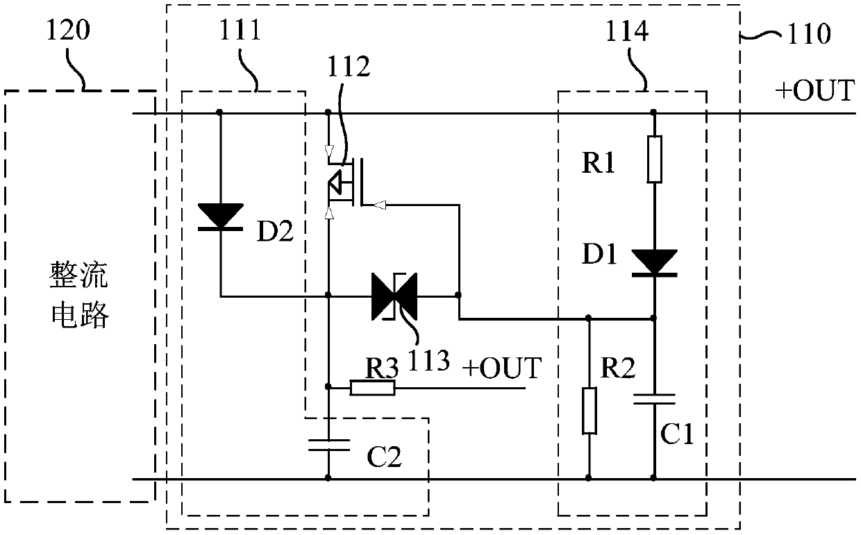
[0020] figure 1 is a schematic diagram of a voltage spike absorbing circuit provided in Embodiment 1 of the present invention, figure 2 It is a schematic structural diagram of a voltage spike absorbing circuit provided in Embodiment 1 of the present invention. The voltage spike absorbing circuit of this embodiment is suitable for absorbing voltage spikes of secondary rectifier tubes of high power density circuits. Such as figure 1 As shown, the specific structure of the voltage spike absorption circuit is as follows:

[0021] A voltage spike absorption circuit 110, comprising a bus peak absorption circuit 111, an energy feedback circuit 112, a protection circuit 113, and an energy absorption circuit 114, wherein,

[0022] The first end of the bus peak absorption circuit 111 is electrically connected to the positive end of the output bus of the rectification circuit 120, and the second end is electrically connected to the negative end of the output bus of the rectification c...

Embodiment 2

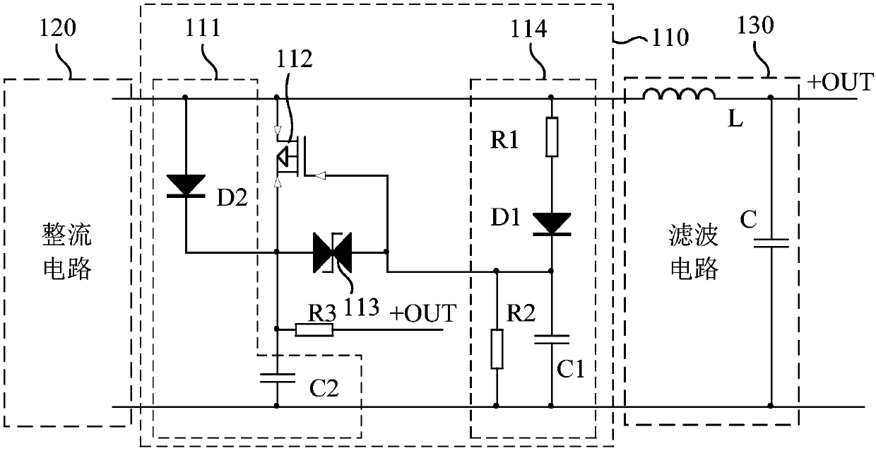
[0045] On the basis of the first embodiment above, the second embodiment of the present invention provides a switching power supply, such as image 3 Shown is a schematic diagram of the structure of a switching power supply.

[0046] A switching power supply, comprising a voltage spike absorbing circuit 110, a rectifying circuit 120 and a filtering circuit 130, wherein,

[0047] The positive end of the output bus of the rectifier circuit 120 is electrically connected to the input end of the voltage spike absorbing circuit 110 and the input end of the filter circuit 130, and the negative end of the output bus bar of the rectifier circuit 120 is electrically connected to the input end of the voltage spike absorbing circuit. The output terminal of 110 is electrically connected with the output terminal of the filter circuit 130 .

[0048] The input end of the voltage spike absorbing circuit 110 is the first end of the voltage spike absorbing circuit 110 , and the output end of t...


PUM


Abstract

The embodiment of the invention discloses a voltage peak absorption circuit. The circuit comprises a bus peak absorption circuit, an energy feedback circuit, a protection circuit and an energy absorption circuit. The first end of the bus peak absorption circuit is electrically connected with the positive end of the output bus of a rectifier circuit. The second end of the bus peak absorption circuit is electrically connected with the negative end of the output bus of the rectifier circuit. The first end of the energy feedback circuit is electrically connected with the positive end of the outputbus of the rectifier circuit. The second end of the energy feedback circuit is electrically connected with the first end of the protection circuit and is electrically connected with the third end ofthe bus peak absorption circuit. The third end of the energy feedback circuit is electrically connected with the second end of the protection circuit. The first end of the energy absorption circuit iselectrically connected with the positive end of the output bus of the rectifier circuit. The second end of the energy absorption circuit is electrically connected with the negative end of the outputbus of the rectifier circuit. The third end of the energy absorption circuit is electrically connected with the third end of the energy feedback circuit. According to the invention, the voltage peak absorption circuit disclosed by the embodiment of the invention is simple in structure, high in absorption efficiency, high in reliability and the like. The voltage peak absorption circuit is suitablefor the voltage peak absorption of the secondary rectifier tube of a high-power-density circuit.

Description

technical field [0001] Embodiments of the present invention relate to the field of switching power supplies, in particular to a voltage spike absorbing circuit. Background technique [0002] With the development of power electronics technology, switching power supplies are tending to be miniaturized and lightweight. In order to reduce the size and weight of the power supply, the switching frequency can be increased. However, with the increase of the switching frequency, the switching loss is also increasing, which brings about the problems of reduced efficiency and serious heat generation. At the same time, due to the high-frequency operation, the influence of parasitic parameters such as leakage inductance and distributed capacitance of the switching transformer cannot be ignored. At the moment of switching transition, the energy charging and discharging of the reactance element causes the power device to bear a lot of heat and electrical stress, and forms an overvoltage....

Claims


Application Information

Patent Timeline
Patent Type & Authority Applications(China)
IPC IPC(8): H02M1/34
CPCH02M1/34H02M1/348
Inventor 王岩
Owner 天津航空机电有限公司
Why Eureka
Try Eureka