Low-noise load driving circuit structure
A load driving circuit, low noise technology, applied in electric light sources, electrical components, adjusting electrical variables, etc., can solve the problems of low power factor, power mismatch, poor stability, etc., to achieve enhanced anti-EMI interference ability, reduce dimming The effect of flickering and good dimming performance
- Summary
- Abstract
- Description
- Claims
- Application Information
AI Technical Summary
Problems solved by technology
Method used
Image
Examples
Embodiment 1
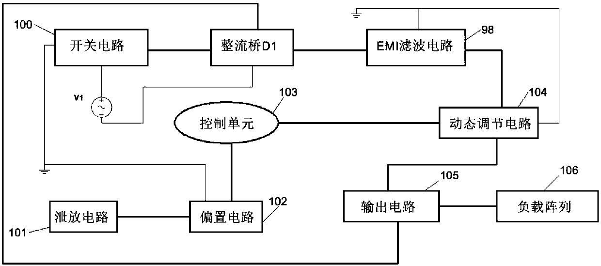
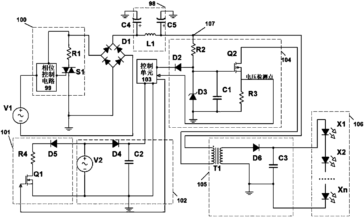
[0025] The dynamic adjustment circuit 104, wherein the zener diode D3 and the first capacitor C1 receive the output voltage of the rectifier bridge D1 through the resistor R2, and accumulate it in the first capacitor C1 to obtain the basis for generating a blocking current; the first field effect transistor Q2 receives the output voltage of the rectifier bridge D1 through the resistor R2. When the received voltage exceeds the reference level, a blocking current is generated to trigger the thyristor switch; the first field effect transistor Q2 has the function of a switch, and here it is in the conduction state.
Embodiment 2
[0027] In the dynamic adjustment circuit 104, the voltage received by the zener diode D3 through the resistor R2 is very high, that is, the voltage value of the voltage node 107 is relatively high, and when it is higher than the reverse conduction voltage of the zener diode D3, the zener diode D3 reverses When the direction is turned on, the first capacitor C1 will be discharged, and the first field effect transistor Q2 will be cut off and in an off state; when the circuit needs to be reset, the control unit 103 resets the dynamic adjustment circuit 104 through the diode D2 to restore the saturation voltage value or below the threshold voltage value.
Embodiment 3
[0029] The control unit 103 detects the source voltage of the first field effect transistor Q1 through a voltage detection point; when the voltage value is abnormal (high or low), the control unit 103 sets the gate voltage of the second field effect transistor Q2 high , so that the switching diode D5 is turned off, the diode D4 is turned on, the second power supply V2 is introduced, the first diode D2 is reversed, and the dynamic adjustment circuit 104 is reset.
PUM
 Abstract
Description
Claims
Application Information

