


Quick Research
Generate reliable direction feasibility study reports for your R&D in just a few steps.

Technical Q&A
Discover and master advanced knowledge NOW. Basics, ideas, possibilities, all at once.

Find Solutions
As an expert in R&D theories, this can generate solutions to your technical problems instantly.

Evaluate Feasibility
Analyze your overall solution with one click, know your potential R&D risks in advance.

Monitor Landscape
Get weekly tech updates, stay abreast of the latest tech innovations and key insights.
ITO conducting film
A conductive film and conductive film technology, applied in the optical field, can solve the problems of poor transmittance, poor chemical stability, low refractive index, etc., and achieve the effect of eliminating obvious etching patterns, good chemical stability and excellent physical properties.
- Summary
- Abstract
- Description
- Claims
- Application Information
AI Technical Summary
Problems solved by technology
Method used
Image

Examples
Embodiment 1
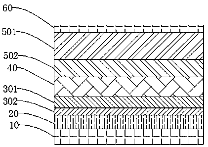
[0023] Such as figure 1 As shown, a kind of ITO conductive film, this conductive film structure is arranged in sequence from top to bottom with protective layer 60, resin matrix 50, silver nano film layer 40, first ITO conductive film layer 301, second ITO conductive film layer 302 , bonding layer 20 and substrate layer 10; The first ITO conductive film layer 301 and the second ITO conductive film layer 302 are transparent conductive film layers, and the refractive index of the two conductive film layers is different, the first ITO conductive film layer The thickness of the ITO conductive film layer 301 is 20-30nm, the thickness of the second ITO conductive film layer 302 is 10-20nm, the thickness of the resin matrix 50 is 110-140mm, and the thickness of the silver nano film layer 40 is 45-20nm. 55nm, the thickness of the bonding layer 20 is 20-50nm.
Embodiment 2
[0025] Such as figure 1 As shown, a kind of ITO conductive film, this conductive film structure is arranged in sequence from top to bottom with protective layer 60, resin matrix 50, silver nano film layer 40, first ITO conductive film layer 301, second ITO conductive film layer 302 , bonding layer 20 and substrate layer 10; The first ITO conductive film layer 301 and the second ITO conductive film layer 302 are transparent conductive film layers, and the refractive index of the two conductive film layers is different, the first ITO conductive film layer The thickness of the ITO conductive film layer 301 is 20-30nm, the thickness of the second ITO conductive film layer 302 is 10-20nm, the thickness of the resin matrix 50 is 110-140mm, and the thickness of the silver nano film layer 40 is 45-20nm. 55nm, the thickness of the bonding layer 20 is 20-50nm.
[0026] Such as figure 1 As shown, the resin matrix 50 is formed by pressing a polyethylene terephthalate resin matrix 501 an...
Embodiment 3
[0028] Such as figure 1 As shown, a kind of ITO conductive film, this conductive film structure is arranged in sequence from top to bottom with protective layer 60, resin matrix 50, silver nano film layer 40, first ITO conductive film layer 301, second ITO conductive film layer 302 , bonding layer 20 and substrate layer 10; The first ITO conductive film layer 301 and the second ITO conductive film layer 302 are transparent conductive film layers, and the refractive index of the two conductive film layers is different, the first ITO conductive film layer The thickness of the ITO conductive film layer 301 is 20-30nm, the thickness of the second ITO conductive film layer 302 is 10-20nm, the thickness of the resin matrix 50 is 110-140mm, and the thickness of the silver nano film layer 40 is 45-20nm. 55nm, the thickness of the bonding layer 20 is 20-50nm.
[0029] Such as figure 1 As shown, the resin matrix 50 is formed by laminating a polyethylene terephthalate resin matrix 501 ...
PUM
| Property | Measurement | Unit |
|---|---|---|
| Thickness | aaaaa | aaaaa |
| Thickness | aaaaa | aaaaa |
| Thickness | aaaaa | aaaaa |
Abstract
Description
Claims
Application Information
 - R&D Engineer
- R&D Manager
- IP Professional
- Industry Leading Data Capabilities
- Powerful AI technology
- Patent DNA Extraction
Browse by: Latest US Patents, China's latest patents, Technical Efficacy Thesaurus, Application Domain, Technology Topic, Popular Technical Reports.
© 2024 PatSnap. All rights reserved.Legal|Privacy policy|Modern Slavery Act Transparency Statement|Sitemap|About US| Contact US: help@patsnap.com