Nano-patterned substrate and manufacturing method thereof

A patterned substrate and manufacturing method technology, applied in the direction of electrical components, circuits, semiconductor devices, etc., can solve the problems of high temperature growth, lattice mismatch, etc.

Pending Publication Date: 2018-03-30
山西中科潞安紫外光电科技有限公司
View PDF9 Cites 9 Cited by
  • Summary
  • Abstract
  • Description
  • Claims
  • Application Information

AI Technical Summary

Problems solved by technology

Existing equipment is often unable to meet the needs of high temperature growth
nPSS substrates (nanoscale patterned substrates) have also appeared in the prior art, but none of the nPSS

Method used


Image

  • Nano-patterned substrate and manufacturing method thereof
  • Nano-patterned substrate and manufacturing method thereof
  • Nano-patterned substrate and manufacturing method thereof

Examples


Embodiment Construction

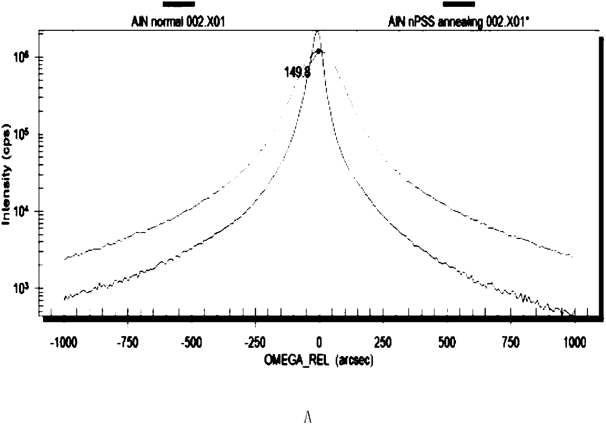
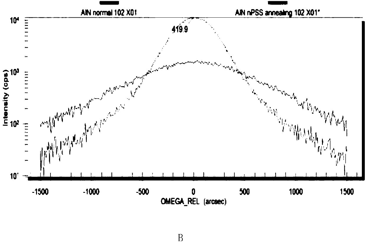
[0012] The specific implementation of this patent will be described in detail below in conjunction with the accompanying drawings. It should be pointed out that this specific implementation is only an example of the preferred technical solution of this patent, and should not be understood as limiting the scope of protection of this patent.

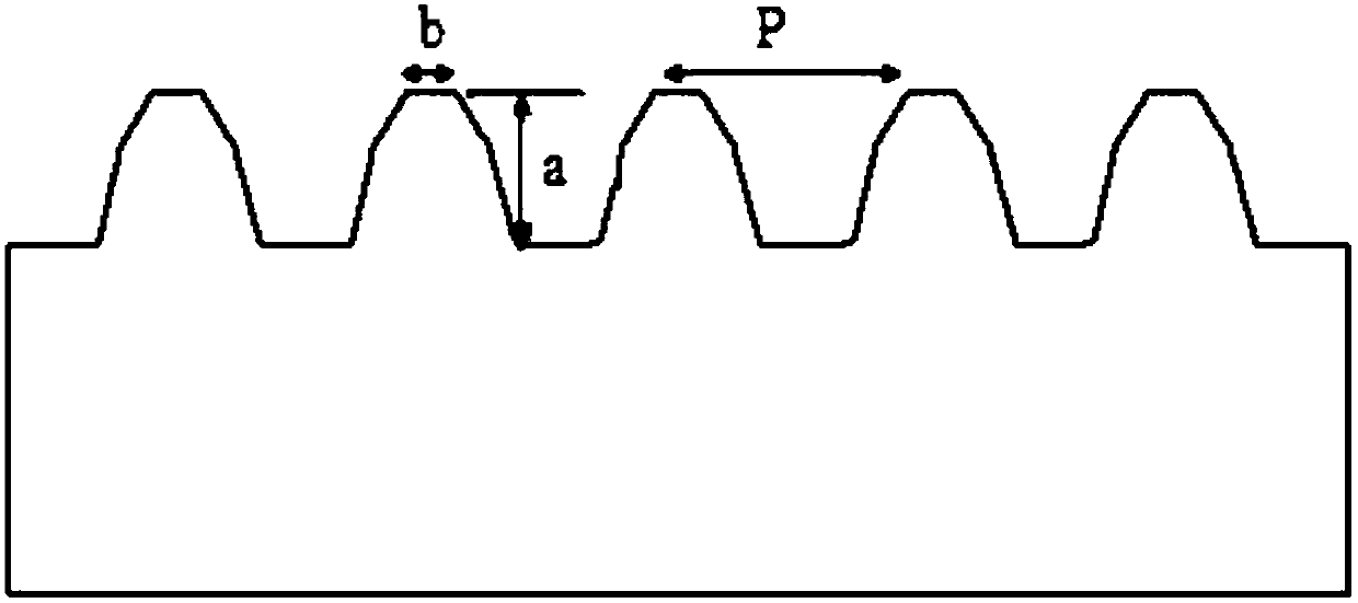
[0013] A method for producing a nanoscale patterned substrate is provided in this specific embodiment, and the method includes the following steps:

[0014] Step 1, first sputtering an AlN layer in the thickness range of 10-800nm ​​on the sapphire plane substrate.

[0015] In this step, a sputtering device is firstly used to grow an AlN layer on the sapphire substrate. The sputtering equipment is preferably used, for example, iTopsA230 aluminum nitride sputtering system, the sputtering temperature of the equipment is 800°C, the high vacuum is on the order of 10-8torr, and 19 pieces of 2-inch sapphire substrates can be sputtered each time. ...


PUM


Abstract

The invention discloses a nano-patterned substrate and a manufacturing method thereof. The nano-patterned substrate is manufactured through sputtering an AlN layer on a sapphire substrate; annealing the AlN layer and then forming a nano-pattern on the annealed AlN layer. The substrate has the characteristics of being simple in manufacturing process and low in cost, the quality of AlN crystal and the light extraction efficiency of a UV-LED (deep ultraviolet light-emitting diode) can be greatly improved, and the nano-patterned substrate is a necessary product for later growth of the deep ultraviolet LED.

Description

technical field [0001] This patent belongs to the field of semiconductor technology, and specifically relates to a nanoscale patterned substrate and a manufacturing method thereof. In particular, an nPSS (nanoscale patterned) substrate for deep ultraviolet light-emitting diodes (UV-LEDs) and a manufacturing method thereof. Background technique [0002] Light-emitting diodes (LEDs) have been widely used in the prior art. In the prior art, because they have been widely used, the deep-ultraviolet light-emitting diode technology belongs to a more advanced direction among all LED technologies. [0003] In the prior art, the production of deep ultraviolet LED chips is usually realized by growing AlN (aluminum nitride) single crystal on a sapphire substrate. However, in the prior art, it is known that it is difficult to grow high-quality AlN single crystals, and it is often difficult to guarantee the efficiency and yield of mass production. First, when growing AlN single crystal,...

Claims


Application Information

Patent Timeline
IPC IPC(8): H01L33/20H01L33/00
CPCH01L33/007H01L33/20
Inventor 王晓东段瑞飞王军喜曾一平付强
Owner 山西中科潞安紫外光电科技有限公司
Why Eureka
Try Eureka