Performance enhancing LED (light emitting diode) preparation method and LED chip

A LED chip and performance technology, applied in the direction of electrical components, circuits, semiconductor devices, etc., can solve the problems of increasing the light output rate of LED chips, and achieve the effects of increasing light output rate, reducing thickness, and reducing light absorption

Active Publication Date: 2018-03-30
XIAMEN CHANGELIGHT CO LTD
View PDF4 Cites 4 Cited by
  • Summary
  • Abstract
  • Description
  • Claims
  • Application Information

AI Technical Summary

Problems solved by technology

[0006] In view of this, the present invention provides an LED preparation method and an LED chip for improving LED performance, so as to solve the problem that the light extraction rate of the LED chip needs to be improved in the prior art

Method used


Image

  • Performance enhancing LED (light emitting diode) preparation method and LED chip
  • Performance enhancing LED (light emitting diode) preparation method and LED chip
  • Performance enhancing LED (light emitting diode) preparation method and LED chip

Examples


preparation example Construction

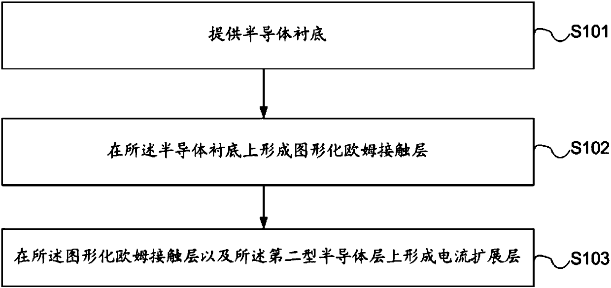
[0048]Based on this, the present invention provides a LED preparation method for improving LED performance, including:

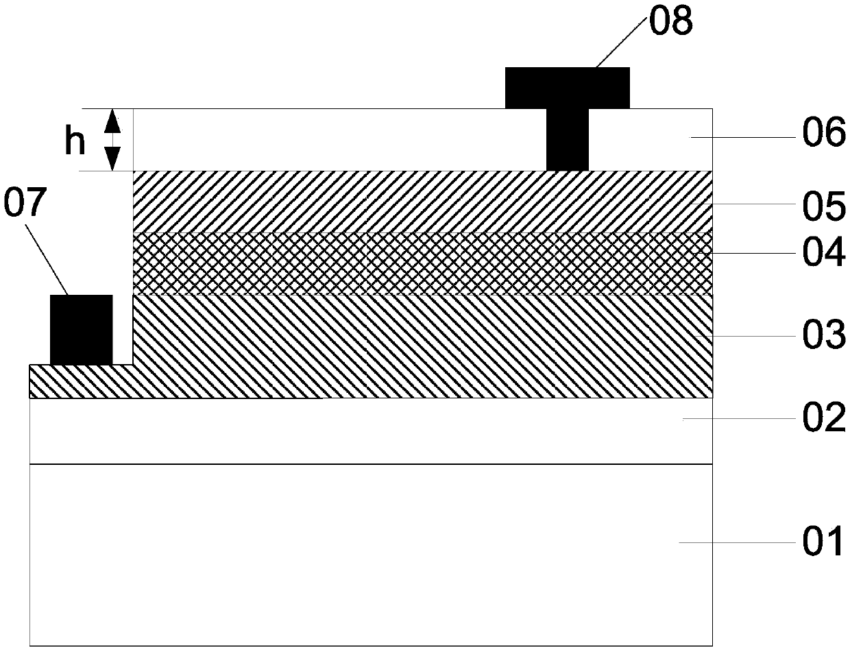
[0049] A semiconductor substrate is provided, the semiconductor substrate at least includes a substrate, and a buffer layer, a first-type semiconductor layer, a multi-quantum well layer, and a second-type semiconductor layer;

[0050] A patterned ohmic contact layer is formed on the semiconductor substrate, and the patterned ohmic contact layer is Ga x In (1-x) N material, where the value range of x is 0.5-1, including 0.5, excluding 1;

[0051] forming a current spreading layer on the patterned ohmic contact layer and the second type semiconductor layer, the current spreading layer comprising: ITO, IZO, IGO or ZnO;

[0052] Wherein, the sum of the thicknesses of the current spreading layer and the ohmic contact layer is less than or equal to

[0053] In the present invention, a patterned ohmic contact layer is used to replace the partial thickness of ...


PUM


Abstract

The invention provides a performance enhancing LED preparation method and an LED chip. The performance enhancing LED preparation method comprises providing a semiconductor substrate, forming a patterned Ohmic contact layer which is made of Ga<x>In<(1-x)>N; forming a current expanding layer on the patterned Ohmic contact layer and a second type semiconductor layer, wherein the total thickness of the current expanding layer and the Ohmic contact layer is smaller than or equal to 1100A. By controlling the composition of In and Ga in the Ohmic contact layer, the patterned Ohmic contact layer can achieve the characteristics of higher transverse conductivity compared with the current expanding layer, good Ohmic contact features with the second type semiconductor layer, an appropriate refractiveindex, and good transmittance effects within the visible spectrum, thereby being capable of replacing a certain thickness of the current expanding layer to achieve a current expanding function and further to improve the light emitting efficiency of the LED chip.

Description

technical field [0001] The invention relates to the technical field of manufacturing semiconductor devices, in particular to an LED preparation method and an LED chip for improving the performance of an LED (Light-Emitting Diode, light-emitting diode). Background technique [0002] LED is called the fourth-generation lighting source or green light source. It has the characteristics of energy saving, environmental protection, long life, and small size. It is widely used in various indications, displays, decorations, backlights, general lighting, and urban night scenes. According to different functions, it can be divided into five categories: information display, signal lights, vehicle lamps, LCD backlight, and general lighting. [0003] A method for improving the luminous efficiency of an LED chip by using a GaP current spreading layer is proposed in the prior art. However, the traditional GaP current spreading layer has the disadvantages of high cost and poor epitaxial qual...

Claims


Application Information

Patent Timeline
Patent Type & Authority Applications(China)
IPC IPC(8): H01L33/38H01L33/14
CPCH01L33/14H01L33/387
Inventor 杨丹杨晓蕾叶佩青翁启伟刘兆
Owner XIAMEN CHANGELIGHT CO LTD
Why Eureka
Try Eureka