OLED device structure and preparation method thereof

A device structure and thin-film technology, which is applied in semiconductor/solid-state device manufacturing, electric solid-state devices, semiconductor devices, etc., can solve the problems affecting the light transmittance of the device, poor barrier performance, and reduced light extraction efficiency of the device, so as to improve the light extraction efficiency , increase the light output efficiency, and the effect of simple production method

Active Publication Date: 2018-03-30
FUZHOU UNIV
View PDF3 Cites 2 Cited by
  • Summary
  • Abstract
  • Description
  • Claims
  • Application Information

AI Technical Summary

Problems solved by technology

The currently used thin film packaging technology overcomes the disadvantages of sealant’s poor barrier performance to water vapor and oxygen, and improves the packaging effect, but the barrier performance to water vapor and oxygen is still not high enough, and the life of the device is still not satisfactory. commercial needs
In addition, the use of organic / inorganic stacked packaging or inorganic / inorganic stacked packaging often affects the light transmittance of the device, resulting in a decrease in the light extraction efficiency of the device, thereby affecting the luminous brightness and luminous efficiency

Method used


Image

  • OLED device structure and preparation method thereof
  • OLED device structure and preparation method thereof
  • OLED device structure and preparation method thereof

Examples


Embodiment 1

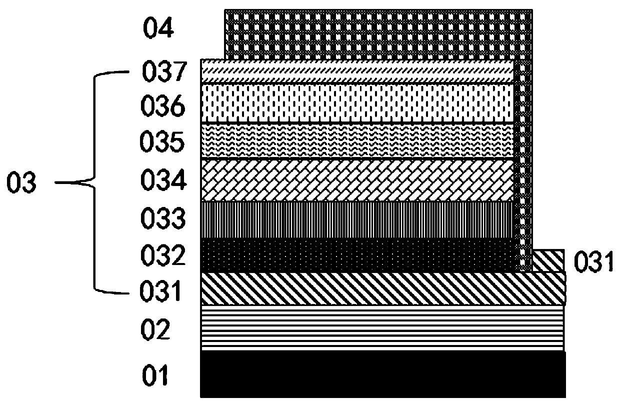
[0040] Such as figure 1 As shown, an OLED device structure is suitable for bottom-emitting OLED devices, including:

[0041] A substrate 01, the substrate 01 comprising a glass substrate or a polymer substrate;

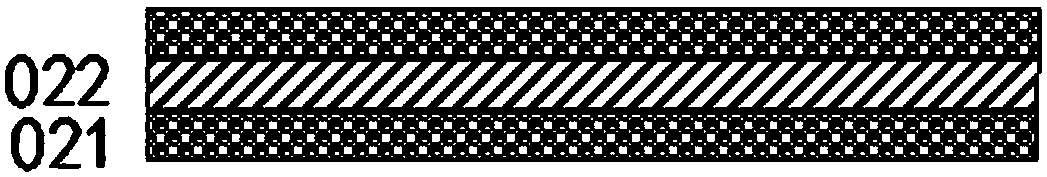
[0042] The first water-oxygen barrier layer 02 with high light transmittance is arranged on the substrate 01, such as figure 2As shown, the first water-oxygen barrier layer 02 is alternately formed by the first low-refractive index film 021 and the first high-refractive index film 022 from bottom to top according to the number of alternating cycles m+0.5, m takes a positive integer, and 0.5 represents The topmost layer of the first water-oxygen barrier layer 02 is the first low-refractive index film 021, that is, an additional layer of low-refractive index film is coated on the film layer to form a low / high / low sandwich structure. The first low-refractive index film 021 The refractive index is smaller than the refractive index of the first high refractive index fil...

Embodiment 2

[0073] The difference between this embodiment and Embodiment 1 is that the positions of the first water-oxygen barrier layer 02 and the second water-oxygen barrier layer 04 are reversed in the structure of the OLED device, and a second water-oxygen barrier layer with high optical reflectivity is arranged above the substrate 01. Oxygen barrier layer 04, the first water and oxygen barrier layer 02 with high light transmittance is arranged on the OLED unit 03, which is suitable for top-emitting OLED devices. The specific structure is:

[0074] The cross-sections of the second water-oxygen barrier layer 04 and the anode 031 are L-shaped, the short side of the second water-oxygen barrier layer 04 is located on the electron injection layer 036, and the long side of the second water-oxygen barrier layer 04 is vertically downward and The long side inner wall of the second water oxygen barrier layer 04 is close to the vertical end faces of the hole injection layer 032, the hole transpo...


PUM


Abstract

The invention relates to an OLED device structure and a preparation method thereof. The OLED device structure comprises a substrate; a first water and oxygen blocking layer which is arranged on the substrate and formed by stacking of two films having high and low refractive index and used for increasing the luminous efficiency of the OLED emitted light and acting as a packaging layer to block water vapor and oxygen; an OLED unit which is arranged on the first water and oxygen blocking layer; and a second water and oxygen blocking layer which is arranged on the OLED unit and formed by stackingof two films having high and low refractive index and used for reflecting the OLED light and acting as a packaging layer to block water vapor and oxygen. Compared with the structures in the prior art,the OLED device structure has complex structure and simple operation, accessible material and substantial effect so that the service life and the light extraction efficiency of the OLED device can beeffectively enhanced.

Description

technical field [0001] The invention relates to the field of organic light emitting diodes, in particular to an OLED device structure and a preparation method. Background technique [0002] As a new generation of display technology, Organic Light Emitting Display (OLED) has the advantages of active light emission, fast response and high contrast. The most attractive thing is that it can be flexible. It has broad application prospects. However, organic light-emitting materials are sensitive to chemical and physical environments, especially to water and oxygen, and the device is prone to aging and has a short service life. Therefore, in order to achieve mass production of OLED devices, the packaging reliability must be solved. [0003] At present, the commonly used packaging methods are (1) The traditional OLED packaging technology generally adds a cover to the device, and attaches a desiccant to the inside of the cover, and then combines the substrate and the cover with a s...

Claims


Application Information

Patent Timeline
Patent Type & Authority Applications(China)
IPC IPC(8): H01L51/50H01L51/52H01L51/56
CPCH10K50/00H10K50/84H10K50/8445H10K71/00
Inventor 周雄图翁雅恋张永爱郭太良李福山杨尊先叶芸
Owner FUZHOU UNIV
Why Eureka
Try Eureka