BGA repair method, apparatus and system

A device pairing and rework station technology, applied in printed circuit repair/correction, printed circuit secondary treatment, post-manufacturing process, etc., can solve problems such as high temperature expansion, affecting BGA chip reliability and life, BGA high temperature bubbles, etc., to achieve Reduce the impact, improve the efficiency of rework work, improve the life and reliability of the effect

Inactive Publication Date: 2018-03-30
GUANGDONG VTRON TECH CO LTD
View PDF3 Cites 0 Cited by
  • Summary
  • Abstract
  • Description
  • Claims
  • Application Information

AI Technical Summary

Problems solved by technology

However, in the current BGA rework process, the BGA is reworked with straight balls and re-soldered to the board, see figure 1 As shown, this method requires three high-temperature (260 degre

Method used


Image

  • BGA repair method, apparatus and system
  • BGA repair method, apparatus and system
  • BGA repair method, apparatus and system

Examples


Embodiment Construction

[0038] The following will clearly and completely describe the technical solutions in the embodiments of the present invention with reference to the accompanying drawings in the embodiments of the present invention. Obviously, the described embodiments are only some, not all, embodiments of the present invention. Based on the embodiments of the present invention, all other embodiments obtained by persons of ordinary skill in the art without making creative efforts belong to the protection scope of the present invention.

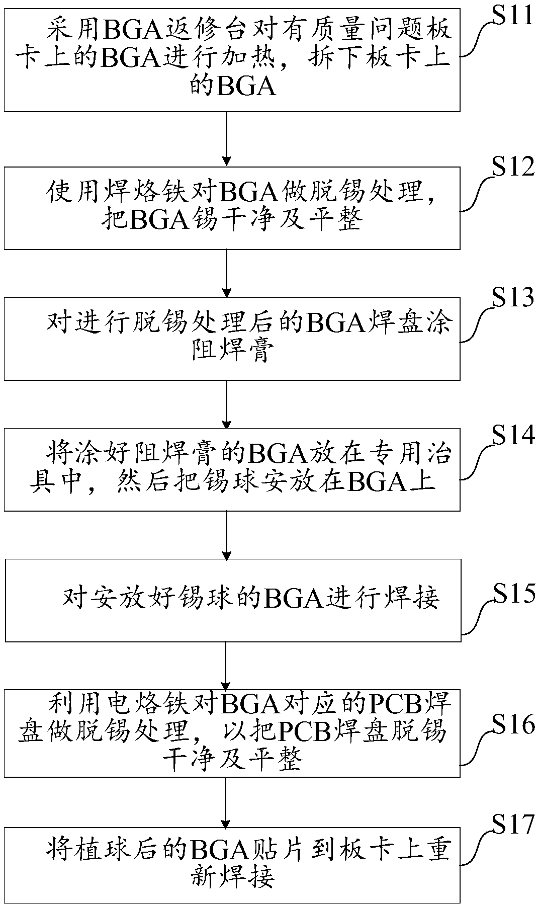
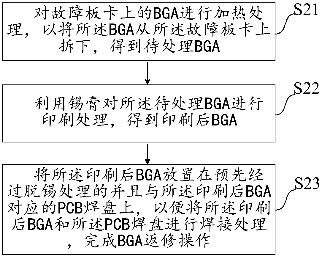
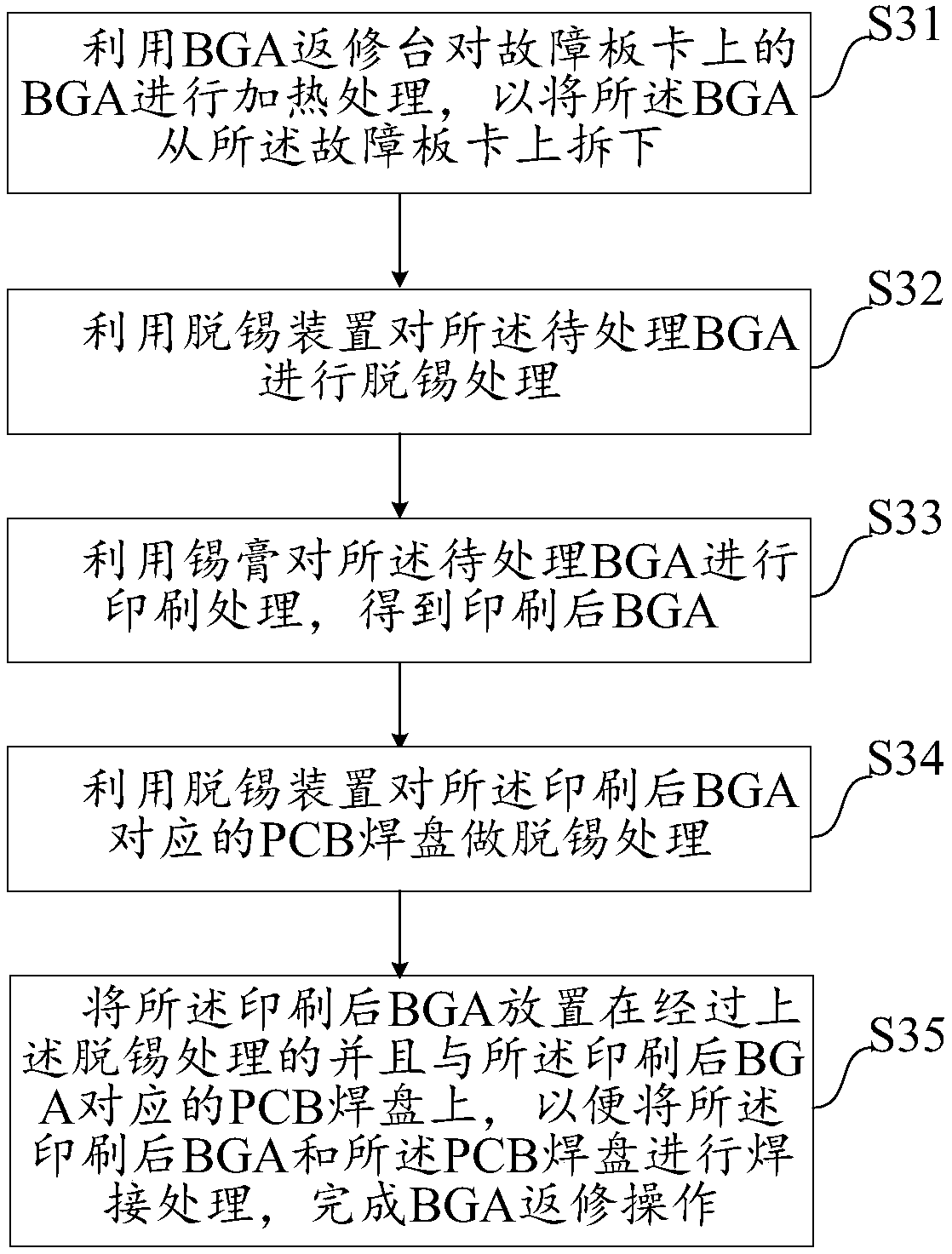
[0039] The embodiment of the present invention discloses a kind of BGA rework method, with reference to figure 2 As shown, the method includes:

[0040] Step S21: performing heat treatment on the BGA on the faulty board to remove the BGA from the faulty board to obtain a BGA to be processed.

[0041] Wherein, the above-mentioned faulty board refers to a problematic PCB board. It can be understood that, in this step, before heating the BGA of the above fault...


PUM


Abstract

The invention discloses a BGA repair method, apparatus and system. The repair method comprises the steps of performing heating treatment on a BGA on a fault board card to detach the BGA from the faultboard card to obtain a to-be-processed BGA; performing printing treatment on the to-be-processed BGA by tin paste to obtain a printed BGA; and putting the printed BGA on a PCB bonding pad which is subjected to de-tinning treatment in advance and corresponding to the printed BGA, so as to perform welding treatment on the printed BGA and the PCB bonding pad to complete BGA repair operation. By virtue of the BGA repair method disclosed in the invention, number of times of high-temperature treatment on the BGA chip can be reduced, thereby lowering influence of a high temperature to the BGA chip,and dramatically prolonging the service life and improving reliability of the BGA chip.

Description

technical field [0001] The invention relates to the technical field of PCB technology, in particular to a BGA rework method, device and system. Background technique [0002] However, with the miniaturization of electronic products, these common packaged components are far from meeting the needs of product design, so a large number of BGA (Ball Grid Array, that is, solder ball array packaging) appear in products, which are placed on the package substrate An array of solder balls is made at the bottom as the I / O terminal of the circuit to be interconnected with a PCB (Printed Circuit Board, ie a printed circuit board). In the SMD (Surface Mounted Devices, surface mount device) process, due to various reasons, there are always some defects, such as empty soldering, short circuit, etc., so it is inevitable that there will be maintenance. For ordinary SMD components, such as chip resistors, chip capacitors, etc., maintenance is relatively easy, and there is basically no need to ...

Claims


Application Information

Patent Timeline
IPC IPC(8): H05K3/22
CPCH05K3/225H05K2203/17
Inventor 黄海兵
Owner GUANGDONG VTRON TECH CO LTD
Why Eureka
Try Eureka