3D NAND preparation method adopting novel channel hole electric connecting layer material and 3D NAND

A technology for electrical connection layers and channels, applied in circuits, electrical components, electrical solid devices, etc., can solve the problems of increasing channel resistivity, limiting conduction capacity, and difficulty in improving channel hole performance, so as to improve stability, Increased read current, good electrical performance

Active Publication Date: 2018-05-04
YANGTZE MEMORY TECH CO LTD
View PDF6 Cites 2 Cited by
  • Summary
  • Abstract
  • Description
  • Claims
  • Application Information

AI Technical Summary

Problems solved by technology

[0007] It can be seen that polysilicon is used as the connection layer material in the prior art; however, as the number of stacked layers increases, the read current (read current) is being seriously concerned, and th

Method used


Image

  • 3D NAND preparation method adopting novel channel hole electric connecting layer material and 3D NAND

Examples


Example Embodiment

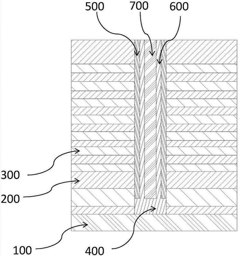
[0031] Hereinafter, exemplary embodiments of the present disclosure will be described in more detail with reference to the accompanying drawings. Although the drawings show exemplary embodiments of the present disclosure, it should be understood that the present disclosure can be implemented in various forms and should not be limited by the embodiments set forth herein. On the contrary, these embodiments are provided to enable a more thorough understanding of the present disclosure and to fully convey the scope of the present disclosure to those skilled in the art.

[0032] For the sake of clarity, not all features of actual embodiments are described. In the following description, well-known functions and structures are not described in detail because they may confuse the present invention due to unnecessary details. It should be considered that in the development of any actual embodiment, a large number of implementation details must be made to achieve the developer's specific ...


PUM


Abstract

The invention provides a 3D NAND preparation method adopting a novel channel hole electric connecting layer material and a 3D NAND. The preparation method comprises the steps of depositing a substratestack structure on a substrate; etching the stack structure to form channel holes, wherein the channel holes are connected to the substrate to form a silicon groove of a certain depth; depositing a graphene epitaxial layer in the silicon groove; forming a channel hole side wall stack structure; etching the stack structure; and depositing a graphene connecting layer, wherein the graphene layer inthe channel hole side wall stack structure is connected with the graphene epitaxial layer through the graphene connecting layer. The thin graphene thin film has very high mobility and mechanical strength, so that the read current can be increased and channel hole structural stability can be improved.

Description

Technical field [0001] The invention relates to the field of semiconductor manufacturing, in particular to a channel hole structure in a 3D NAND flash memory structure and a preparation method thereof. Background technique [0002] With the development of planar flash memory, the semiconductor production process has made tremendous progress. But in recent years, the development of planar flash memory has encountered various challenges: physical limits, limits of existing development technology, and limits of storage electron density. In this context, in order to solve the difficulties encountered by planar flash memory and the lowest production cost of unit memory cells, various three-dimensional (3D) flash memory structures have emerged, such as 3D NOR (3D or non) flash memory. And 3D NAND (3D NAND) flash memory. At present, in the development process of 3D NAND, with the increase in the number of stacked layers, higher requirements are put forward for preparation processes su...

Claims


Application Information

Patent Timeline
IPC IPC(8): H01L27/1157H01L27/11578
CPCH10B43/35H10B43/20
Inventor 方振
Owner YANGTZE MEMORY TECH CO LTD
Why Eureka
Try Eureka