Quantum chip and method capable of coupling multiple quantum bits by using regulatable quantum data bus

A data bus and qubit technology, applied to waveguide devices, electrical components, waveguides, etc., can solve the problems of redundant hardware systems and high resource consumption, and achieve optimal structural design, simplified structural design, and convenient control and signal processing. Effect

Active Publication Date: 2018-05-04
ORIGIN QUANTUM COMPUTING TECH (HEFEI) CO LTD
View PDF6 Cites 26 Cited by
  • Summary
  • Abstract
  • Description
  • Claims
  • Application Information

AI Technical Summary

Problems solved by technology

[0006] Aiming at the problem that the existing multi-qubit chip hardware system is complicated and consumes a lot of resources, the present invention provides a quantum chip that uses an adjustable quantum data bus to couple multiple qubits, which can control and read signals with specified frequencies and corresponding The qubit / reading resonant cavity is matched, which greatly facilitates the regulation and signal processing of multi-qubit chips

Method used


Image

  • Quantum chip and method capable of coupling multiple quantum bits by using regulatable quantum data bus
  • Quantum chip and method capable of coupling multiple quantum bits by using regulatable quantum data bus
  • Quantum chip and method capable of coupling multiple quantum bits by using regulatable quantum data bus

Examples


Embodiment 1

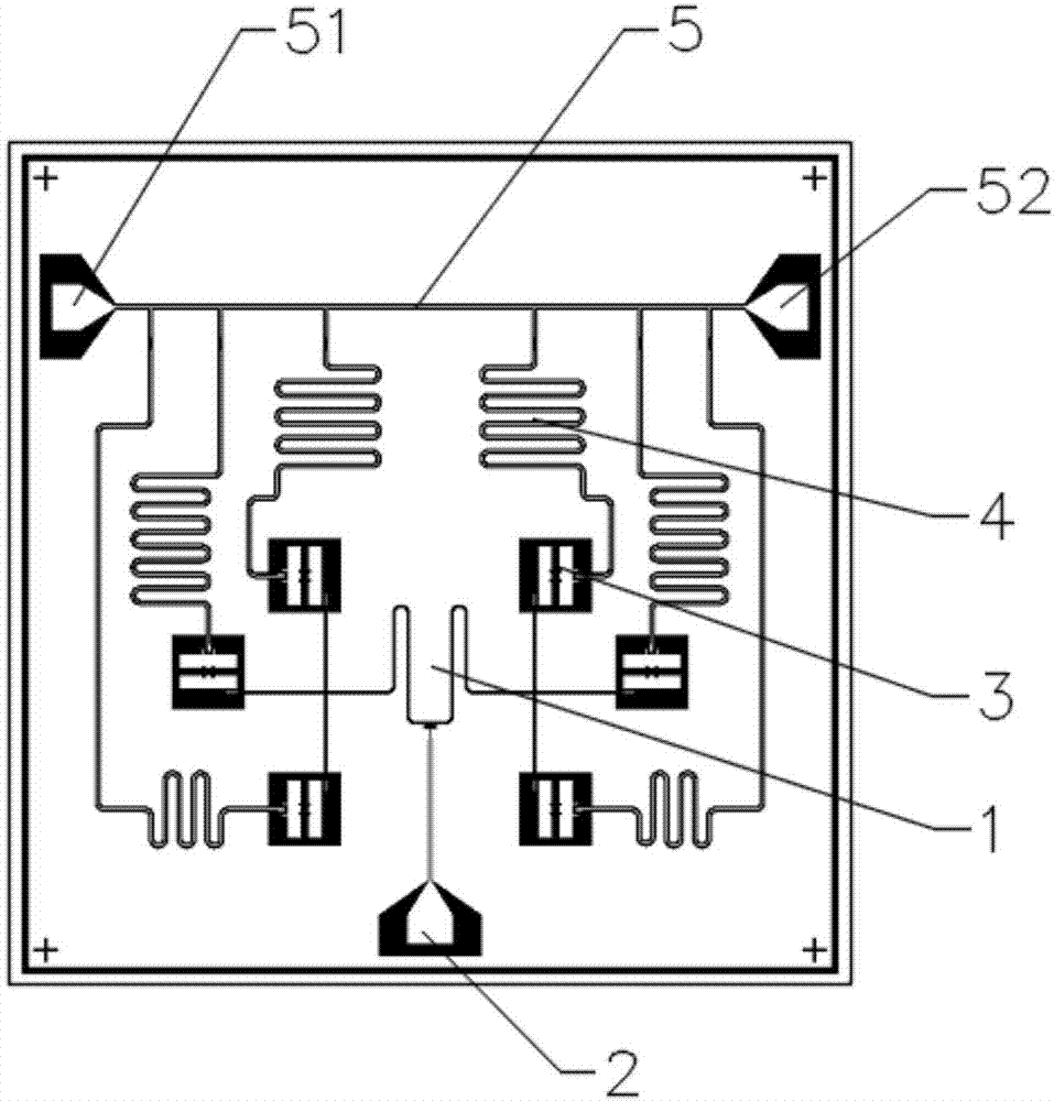
[0044] Such as figure 1 , figure 2 and image 3 As shown, a quantum chip that uses an adjustable quantum data bus to couple multiple qubits includes a substrate and a classical data bus 5 and six qubits 3 printed on the substrate. The classical data bus 5 includes input port 51 and output port 52; also includes:

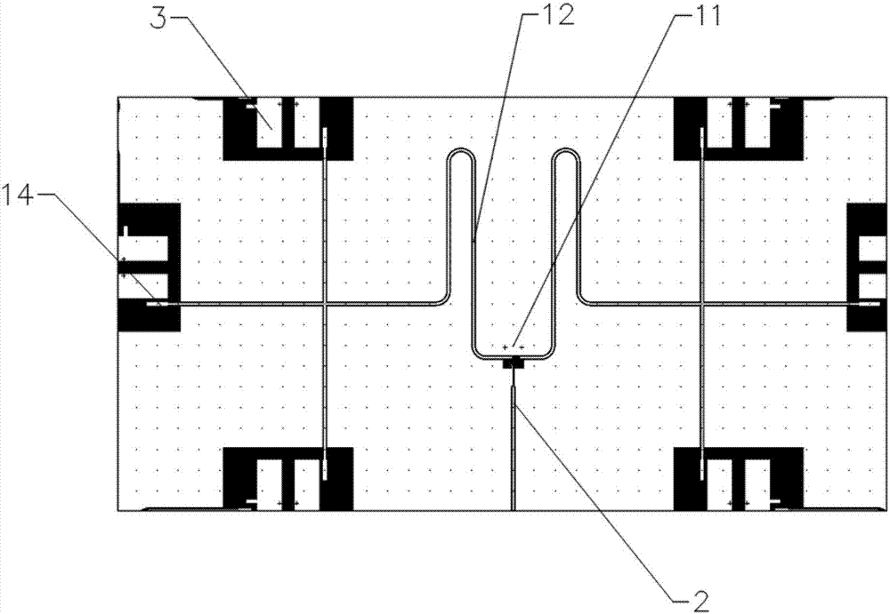
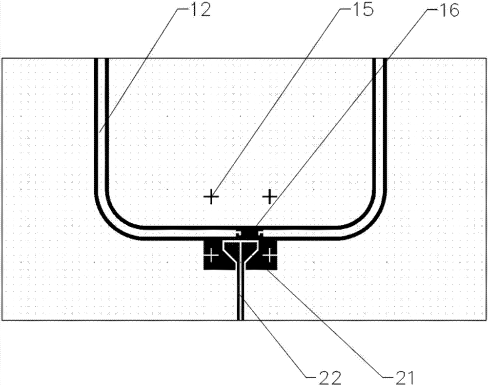
[0045] The adjustable quantum data bus 1, the adjustable quantum data bus 1 is printed on the substrate, and the qubits 3 are connected through the coupling structure 14, which is a centrosymmetric structure, including a half-wavelength coplanar waveguide resonant cavity 12 and a resonance Cavity resonant frequency adjustment element 11; the resonant cavity resonant frequency adjustment element 11 is arranged at the center of the adjustable quantum data bus 1; in this embodiment, the coupling structure 14 is a capacitive coupling structure;

[0046]The number of qubit read resonators 4 corresponds to the number of qubits 3, so that each qubit 3 is assigned an ind...

Embodiment 2

[0072] Such as Figure 4 , Figure 5 and Figure 6 As shown, a quantum chip that uses an adjustable quantum data bus to couple multiple qubits is basically the same as Embodiment 1, the difference is that the resonant cavity resonant frequency adjustment element 11 of the adjustable quantum data bus 1, that is, the adjustable inductance The structure is further designed in the form of qubits, which can be used to impose additional control degrees of freedom. The connection relationship and working principle of its components are the same as those of Embodiment 1, and can produce the same technical effects as Embodiment 1.


PUM


Abstract

The present invention provides a quantum chip and a method capable of coupling multiple quantum bits by using a regulatable quantum data bus, pertaining to the field of microwave circuits. The quantumchip comprises a substrate, and a classic data bus and the quantum bits printed on the substrate, and the classic data bus comprises an input port and an output port. The regulatable quantum data buscomprises a half-wavelength coplanar waveguide resonant cavity and a resonant cavity resonant frequency regulating component, the regulatable quantum data bus is connected with the quantum bits via coupling structures, and the resonant cavity resonant frequency regulating component is arranged at the central position of the regulatable quantum data bus. One end of each reading resonant cavity ofeach quantum bit is connected with the classic data bus, and the other end of each reading resonant cavity is connected with the corresponding quantum bit. The quantum chip and the method can match signals of a specified frequency in regulating/ reading signals with the corresponding quantum bits/ reading resonant cavities, and thus the quantum chip and the method can greatly facilitate the regulation and the signal processing of a multiple quantum bit chip.

Description

technical field [0001] The invention belongs to the field of microwave circuits, and in particular relates to a quantum chip using an adjustable quantum data bus to couple multiple qubits. Background technique [0002] At present, the mainstream solid-state quantum chip research teams in the world have entered the development stage of multi-qubit integration. Many top teams have successively proposed their own integration solutions. Each integration scheme has its own defects, which are mainly reflected in two aspects. One is that the increase in chip complexity leads to a decrease in its performance, and the other is that the increase in the number of qubits increases the demand for hardware measurement and control systems. Especially for the latter, if each qubit requires a separate reading and control channel, then the scale of the entire quantum chip measurement and control platform must be increased in proportion, consuming a lot of resources and manpower. We hope to ...

Claims


Application Information

Patent Timeline
Patent Type & Authority Applications(China)
IPC IPC(8): H01P3/00H01P7/06
CPCH01P3/00H01P7/065
Inventor 杨夏朱美珍
Owner ORIGIN QUANTUM COMPUTING TECH (HEFEI) CO LTD
Why Eureka
Try Eureka