Electrostatic protection circuit applied to depth sensor, and depth sensor
A depth sensor and electrostatic protection technology, applied in the field of depth sensors, can solve problems such as inability to protect static electricity, lack of ESD reliability, and inability to effectively protect products, and achieve the effects of low cost, simple structure, good reliability and durability
- Summary
- Abstract
- Description
- Claims
- Application Information
AI Technical Summary
Problems solved by technology
Method used
Image
Examples
Embodiment Construction
[0034] In order to have a clearer understanding of the technical features, purposes and effects of the present invention, the specific implementation manners of the present invention will now be described in detail with reference to the accompanying drawings.
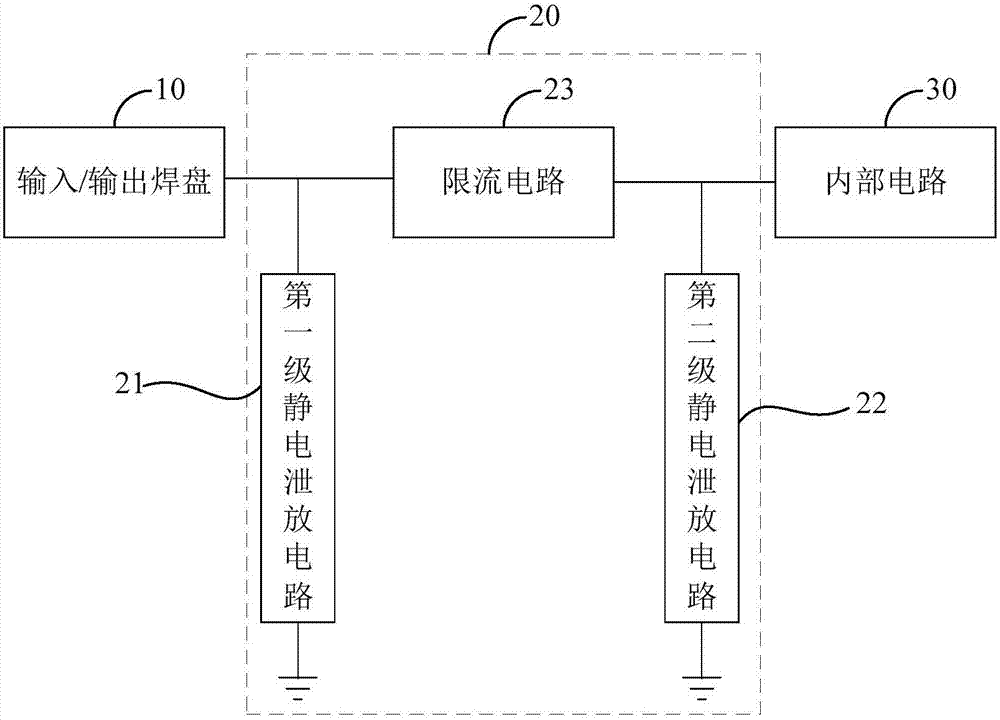
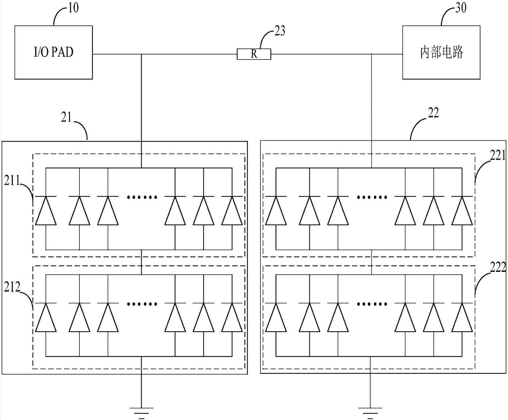
[0035] The electrostatic protection circuit of the embodiment of the present invention can be applied to a depth sensor, especially to a high-voltage TOF (Time of flight) depth sensor chip with a 0.13-micron process. In the electrostatic protection circuit of the embodiment of the present invention, under the normal working conditions of the chip, the electrostatic protection circuit is in the off state, which has no effect on the normal operation of the chip. When a high-voltage and high-current electrostatic input occurs at the input / output pad of the chip , that is, the electrostatic current generated can be quickly suppressed, so that the electrostatic current generated by the high voltage does not flow through the i...
PUM
 Abstract
Description
Claims
Application Information

