Semiconductor device package structure and package method

A device packaging and semiconductor technology, which is applied in the fields of semiconductor devices, semiconductor/solid-state device manufacturing, and semiconductor/solid-state device parts, etc. Low production cost and small package size

Inactive Publication Date: 2018-05-08
SHANGHAI XIANFANG SEMICON CO LTD
View PDF6 Cites 9 Cited by
  • Summary
  • Abstract
  • Description
  • Claims
  • Application Information

AI Technical Summary

Problems solved by technology

[0005] Therefore, the technical problem to be solved by the present invention is to overcome the defects of complex manufacturing process and high production cost of the multi-chip stacked recombined wafer packaging structure in the prior art

Method used


Image

  • Semiconductor device package structure and package method
  • Semiconductor device package structure and package method
  • Semiconductor device package structure and package method

Examples


Embodiment 1

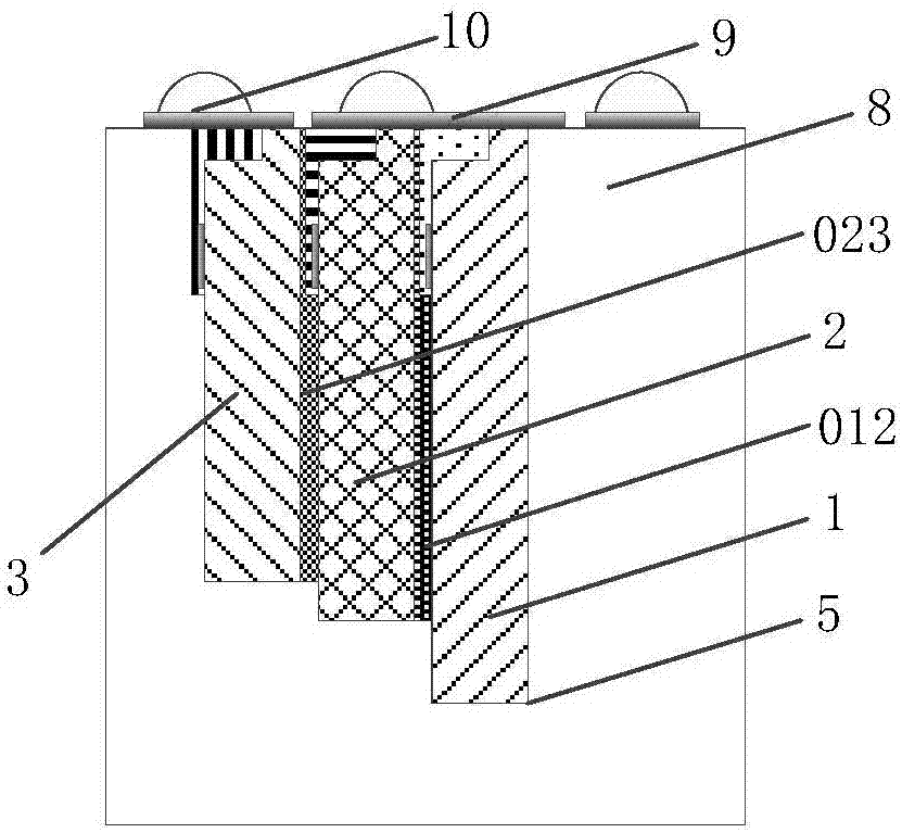
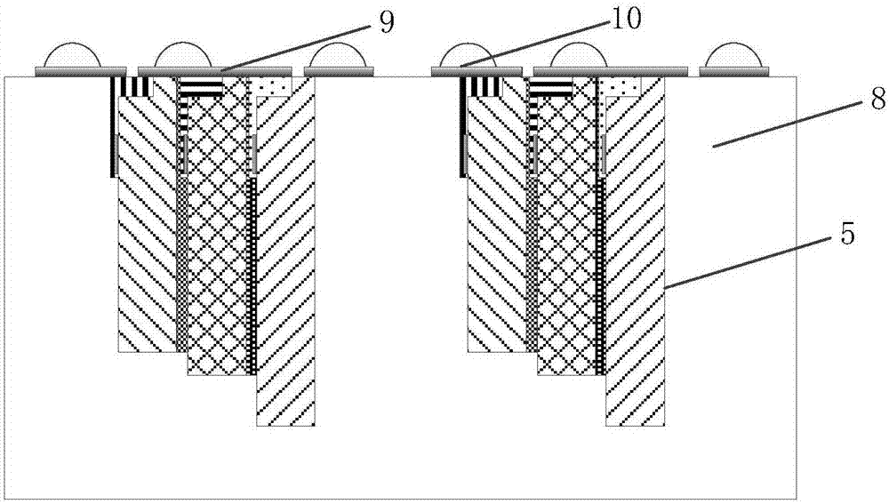
[0034] This embodiment provides a semiconductor device packaging structure, such as figure 1 As shown, it includes: a chipset 5, the chipset 5 is arranged in the encapsulation layer 8, the chipset 5 includes a plurality of chips connected in the vertical direction, and the leads of each chip in the plurality of chips are all located in the chipset 5 On the side wall, the side wall is exposed outside the encapsulation layer 8; the redistribution layer 9 is arranged on the side wall and the encapsulation layer 8, and is connected to the lead on the side wall; the bump 10 is arranged on the redistribution layer 9, and Rewiring layer 9 connections. Each chipset 5 is obtained by cutting a plurality of chipsets placed vertically above the carrier, wherein the side walls are connected to the carrier. In this embodiment, the chipset 5 includes a chipset, such as figure 1 shown; of course, in other embodiments, the chipset 5 can also include multiple chipsets, such as two chipsets, s...

Embodiment 2

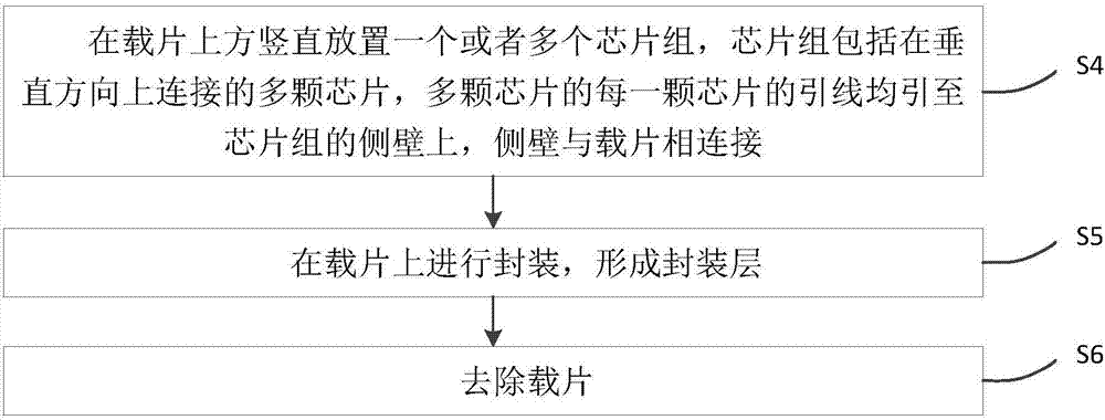
[0039] This embodiment provides a semiconductor device packaging method, the flow chart is as follows image 3 Shown; As a preferred solution of this embodiment, the flow chart is as follows Figure 4 shown, including the following steps:

[0040] S1: lead the leads of each of the chips to the sidewall. In this embodiment, there are three chips, which are the first chip 1, the second chip 2 and the third chip 3 in sequence. The first chip 1 is cut from the first wafer 01, and the second chip 2 is cut from the first wafer 01. Two wafers are cut, and the third chip 3 is cut from the third wafer; of course, in other embodiments, the number of chips can also be two, four or even more, and it can be reasonably set as required. Can. In this embodiment, the three chips are different chips, and of course, in other embodiments, they may also be the same chip, which can be reasonably set as required.

[0041] Taking the first chip 1 obtained by cutting the first wafer 01 as an examp...


PUM


Abstract

The invention provides a semiconductor device package structure and package method. The package structure comprises a chip group, wherein the chip group is arranged in a package layer and comprises aplurality of chips, the plurality of chips are connected in a perpendicular direction, a lead of each chip in the plurality of chips is arranged on a side wall of the chip group, and a side wall is exposed out of the package layer. The lead of each chip in the chip group is connected to the side wall of the chip group from a bonding pad, the lead is connected from the side wall, the line distanceamong chips is reduced, so that a signal is more rapidly transferred, and various TSV double-side processes are prevented; and the semiconductor device is high in reliability, small in package size, good in integral performance, simple in fabrication process and high in production efficiency.

Description

technical field [0001] The invention relates to the field of wafer packaging, in particular to a semiconductor device packaging structure and packaging method. Background technique [0002] Currently, a reconstituted wafer method includes placing a cut semiconductor chip in an opening arranged on a frame, and forming a reconstituted wafer by filling the opening with a mold compound, the molding compound is formed around the chip, and a finished die is formed within the reconstituted wafer, separating the finished die from the frame. [0003] Chip stacking is to stack two or more chips in the Z direction. The interconnection methods between chips are usually wire bonding (Wire Bonding, abbreviated as WB), flip chip (Flip Chip, abbreviated as FC) and Silicon Communications. Holes (ThroughSilicon Via, abbreviated as TSV). [0004] Compared with single-chip packaging and stacking, reorganizing wafer packaging after stacking multiple chips has the advantages of less process, lo...

Claims


Application Information

Patent Timeline
Patent Type & Authority Applications(China)
IPC IPC(8): H01L25/065H01L23/48H01L23/31H01L21/50H01L21/56
CPCH01L25/0655H01L21/50H01L21/56H01L23/3157H01L23/48H01L2224/18H01L2924/181H01L2224/32145H01L2224/12105H01L2224/96H01L2924/00012
Inventor 任玉龙孙鹏
Owner SHANGHAI XIANFANG SEMICON CO LTD
Why Eureka
Try Eureka