
Liquid crystal display mother board and manufacturing method thereof

A liquid crystal display and motherboard technology, which is applied in nonlinear optics, instruments, optics, etc., can solve the problems of difficult control of frame glue width precision, hinder product diversification design, limit substrate utilization rate, etc., and improve product cycle time time, is conducive to rapid development, and occupies a small area

Inactive Publication Date: 2018-05-15
TCL CHINA STAR OPTOELECTRONICS TECH CO LTD
View PDF3 Cites 4 Cited by
  • Summary
  • Abstract
  • Description
  • Claims
  • Application Information

AI Technical Summary

Problems solved by technology

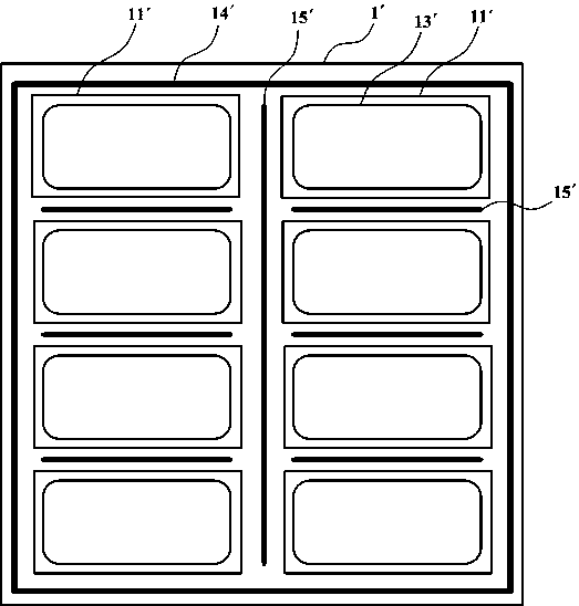
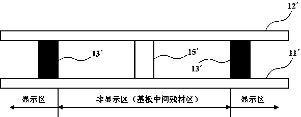
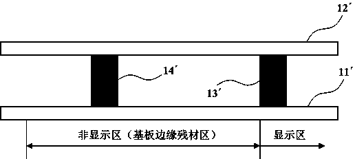
[0003] However, the virtual sealant 15´ and the ring sealant 14´ on the glass substrate 1´ are numerous and complex, so the ODF process takes a lot of time to coat these two types of sealant, and due to the Because the width accuracy is not easy to control and other reasons, a large space must be reserved on the substrate for the footprints of these two frame glues, which limits the utilization rate of the substrate and hinders the diversified design of products

Method used


Image

  • Liquid crystal display mother board and manufacturing method thereof
  • Liquid crystal display mother board and manufacturing method thereof
  • Liquid crystal display mother board and manufacturing method thereof

Examples


Embodiment 1

[0041] Corresponding to Embodiment 1 of the present invention, Embodiment 2 of the present invention provides a method for manufacturing a liquid crystal display motherboard, including:

[0042] An array substrate and a color filter substrate arranged opposite to each other are provided, and a plurality of TFT substrates arranged in an array are formed on the array substrate;

[0043] An engaging structure made of a photoresist material is provided between the array substrate and the color filter substrate, and the engaging structure is used to replace the virtual sealing frame and the ring sealing frame to support the liquid crystal display motherboard The non-display area and the residual material connecting the array substrate and the color filter substrate.

[0044] Wherein, the engaging structure is manufactured in the same manufacturing process of the array substrate or the color filter substrate as the color resist or black matrix.

[0045] From the above description, ...


PUM


Abstract

The invention provides a liquid crystal display mother board and a manufacturing method thereof. The liquid crystal display mother board comprises an array substrate and a color film substrate which are oppositely arranged, a clamping structure which is arranged between the array substrate, the color film substrate and is made of a photoresist and a residual material supporting the non-display region of the liquid crystal display mother board and connecting the array substrate and the color film substrate, wherein the array substrate is provided with a plurality of TFT substrates arranged in an arrayed mode; the clamping structure is used for replacing a virtual sealing frame adhesive and an annular sealing frame adhesive. The clamping structure made of the photoresist replaces the commonvirtual sealing frame adhesive and the annular sealing frame adhesive to achieve the same effect, and due to the fact that the clamping structure can be manufactured through a common exposure technology in the manufacturing process of the array substrate or the color film substrate, the requirement for the manufacturing process of coating the virtual sealing frame adhesive and the annular sealingframe adhesive is lowered, and the product pitch time is shortened; the clamping structure is manufactured in an exposure mode, the precision is higher, the floor area is small, and therefore the product cost is lowered.

Description

technical field [0001] The invention relates to the technical field of screen display, in particular to a liquid crystal display motherboard and a manufacturing method thereof. Background technique [0002] The liquid crystal display motherboard is formed by combining a thin film transistor (TFT) substrate and a color filter (Color Filter, CF) substrate, and injecting liquid crystal between the two substrates using the One Drop Filling (ODF) process. There are generally multiple TFT substrates 11´ distributed on the large-size glass substrate 1´, and the TFT and CF substrates are bonded by frame glue, such as figure 1 As shown, in addition to the main seal (Main seal) 13´ in the TFT substrate 11´, there is also a Dummey seal (Dummey seal) 15´ between the TFT substrates 11´, and a ring along the edge of the glass substrate 1´. Loop seal 14´. Such as figure 2 , image 3 As shown, the role of virtual sealing frame glue 15´ and ring sealing frame glue 14´ is mainly to suppo...

Claims


Application Information

Patent Timeline
Patent Type & Authority Applications(China)
IPC IPC(8): G02F1/1339G02F1/1335
CPCG02F1/133512G02F1/133514G02F1/1339
Inventor 罗忠云
Owner TCL CHINA STAR OPTOELECTRONICS TECH CO LTD
Learn More