An optimization method for misjudgment of line marks by silicon wafer particle dust

An optimization method and technology of silicon wafers, applied in the direction of optical testing flaws/defects, etc., can solve problems such as large technical errors, achieve the effect of high degree of automation, strong practicability, and ensure scanning accuracy

Active Publication Date: 2021-04-02
阜宁协鑫光伏科技有限公司
View PDF13 Cites 0 Cited by
  • Summary
  • Abstract
  • Description
  • Claims
  • Application Information

AI Technical Summary

Problems solved by technology

The original technical error is large, these are the places we need to change

Method used


Image

  • An optimization method for misjudgment of line marks by silicon wafer particle dust
  • An optimization method for misjudgment of line marks by silicon wafer particle dust
  • An optimization method for misjudgment of line marks by silicon wafer particle dust

Examples


Embodiment 1

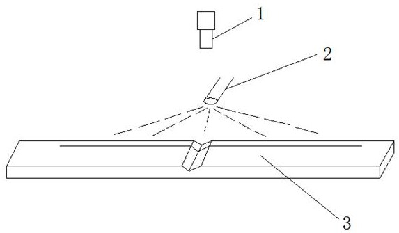
[0018] A method for optimizing silicon chip particle dust misjudgment line marks, the specific steps of the silicon chip particle dust misjudgment line mark optimization method are as follows:

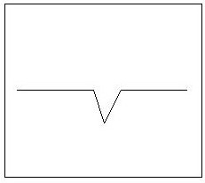
[0019] S1: The 3D laser scanner performs laser scanning on the silicon wafer, and 12 laser lines measure the line marks on the upper and lower sides of the silicon wafer respectively;

[0020] S2: The 3D laser scanner transmits the scanning information to the digital signal processor for analysis and processing to obtain the deviation data of the 12 laser lines at the line marks, and collects the data at the same time;

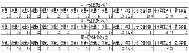
[0021] S3: The digital signal processor automatically numbers the data of the 12 laser lines, respectively numbered as measurement 1, measurement 2, measurement 3, measurement 4, measurement 5, measurement 6, measurement 7, measurement 8, measurement 9, measurement 10, measurement 11 and measure 12, obtain data 13, 12, 13, 12, 11, 12, 33, 13, 12, 44, 12 and 13, and cal...

Embodiment 2

[0025] A method for optimizing silicon chip particle dust misjudgment line marks, the specific steps of the silicon chip particle dust misjudgment line mark optimization method are as follows:

[0026] S1: The 3D laser scanner performs laser scanning on the silicon wafer, and 12 laser lines measure the line marks on the upper and lower sides of the silicon wafer respectively;

[0027] S2: The 3D laser scanner transmits the scanning information to the digital signal processor for analysis and processing to obtain the deviation data of the 12 laser lines at the line marks, and collects the data at the same time;

[0028] S3: The digital signal processor automatically numbers the data of the 12 laser lines, respectively numbered as measurement 1, measurement 2, measurement 3, measurement 4, measurement 5, measurement 6, measurement 7, measurement 8, measurement 9, measurement 10, measurement 11 and measure 12, obtain data 13, 12, 13, 12, 11, 12, 12, 13, 12, 44, 12 and 13, and cal...

Embodiment 3

[0032] A method for optimizing silicon chip particle dust misjudgment line marks, the specific steps of the silicon chip particle dust misjudgment line mark optimization method are as follows:

[0033] S1: The 3D laser scanner performs laser scanning on the silicon wafer, and 12 laser lines measure the line marks on the upper and lower sides of the silicon wafer respectively;

[0034] S2: The 3D laser scanner transmits the scanning information to the digital signal processor for analysis and processing to obtain the deviation data of the 12 laser lines at the line marks, and collects the data at the same time;

[0035] S3: The digital signal processor automatically numbers the data of the 12 laser lines, respectively numbered as measurement 1, measurement 2, measurement 3, measurement 4, measurement 5, measurement 6, measurement 7, measurement 8, measurement 9, measurement 10, measurement 11 and measure 12, obtain data 13, 12, 13, 12, 11, 12, 12, 13, 12, 13, 12 and 13, and cal...


PUM


Abstract

The invention discloses an optimization scheme for misjudgment of silicon chip particle dust as a line mark. The specific steps of the optimization scheme are as follows: S1, using a three-dimensionallaser scanner to perform laser scanning on a silicon chip; S2, using a digital signal processor to analyze and process scan information; and S3, using the digital signal processor for automatically numbering data of 12 laser lines. Compared with the prior art, the beneficial effects of the optimization scheme are as follows, the three-dimensional laser scanner performs laser scanning on the silicon chip to effectively guarantee scanning accuracy, and at the same time, the digital signal processor calculates the average value of 12 measurement locations in one line mark based on the scanning information, according to the average value, whether dust exist on the silicon chip can be judged, and the optimization scheme has the advantages of high degree of automation, accurate measurement, small error, and strong practicality.

Description

technical field [0001] The invention relates to the technical field of silicon wafers, in particular to a method for optimizing silicon wafer particle dust misjudgment line marks. Background technique [0002] Photovoltaic power generation is mainly a new technology that converts light energy into electrical energy through the principle of photovoltaic effect. Photovoltaic technology is a new idea for human beings to further utilize solar energy resources, and its development greatly facilitates human life. The foundation of the photovoltaic industry is the silicon material industry, silicon single crystal material is the foundation of the semiconductor industry, and material processing is the foundation of the foundation. The production of silicon wafers is mainly realized by wire cutting of SiC (silicon carbide) free abrasives. Silicon ingot slicing is the most basic process in photovoltaic technology. Lithography, etc.) play a vital role. In the process of silicon wafe...

Claims


Application Information

Patent Timeline
Patent Type & Authority Patents(China)
IPC IPC(8): G01N21/94
CPCG01N21/94
Inventor 瞿述良蒋旭郝燕云陈训亮程燕群
Owner 阜宁协鑫光伏科技有限公司
Why Eureka
Try Eureka