Preparation method of TEM sample of nickel metal silicide

A metal silicide and sample technology, which is applied in the field of transmission electron microscope sample preparation, can solve problems such as inability to distinguish nickel metal silicides, reduce machine use efficiency, and fail to realize structural defect analysis of nickel metal silicides. Effect of reducing observation cost and shortening observation time

Active Publication Date: 2018-06-01
SHANGHAI HUALI MICROELECTRONICS CORP
View PDF7 Cites 3 Cited by
  • Summary
  • Abstract
  • Description
  • Claims
  • Application Information

AI Technical Summary

Problems solved by technology

Depend on figure 1 As can be seen from the TEM photographs, it can only be seen that the nickel metal silicide is located within the area of ​​the dotted circle 104, but the nickel metal silicide cannot be distinguished from the silicon substrate 101, so it is impossible to realize the detection of the nickel

Method used


Image

  • Preparation method of TEM sample of nickel metal silicide
  • Preparation method of TEM sample of nickel metal silicide
  • Preparation method of TEM sample of nickel metal silicide

Examples


Embodiment Construction

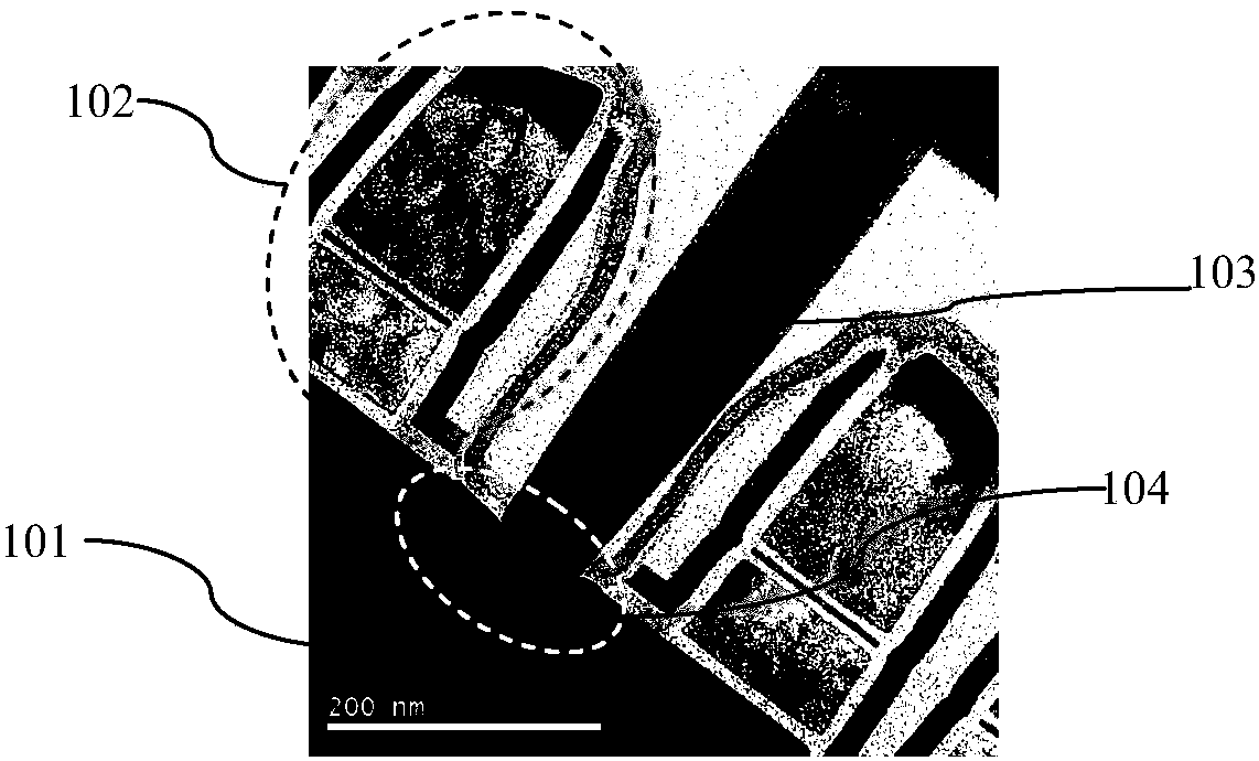
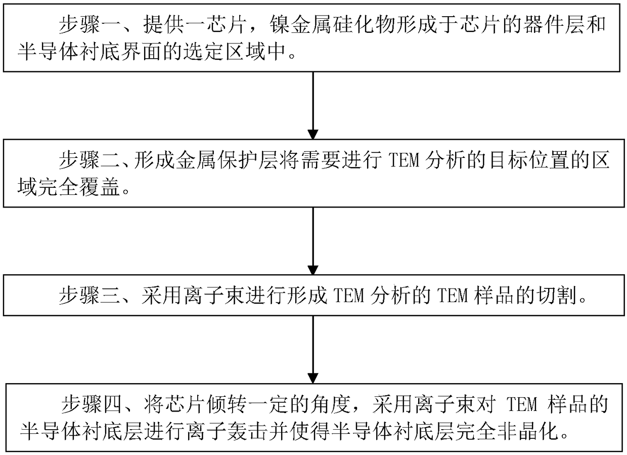
[0030] like figure 2 As shown, it is a flow chart of the preparation method of the TEM sample 201 of nickel metal silicide according to the embodiment of the present invention; 3A to 3C As shown, it is a flow chart of the method of the embodiment of the present invention; the preparation method of the TEM sample 201 of nickel metal silicide in the embodiment of the present invention includes the following steps:

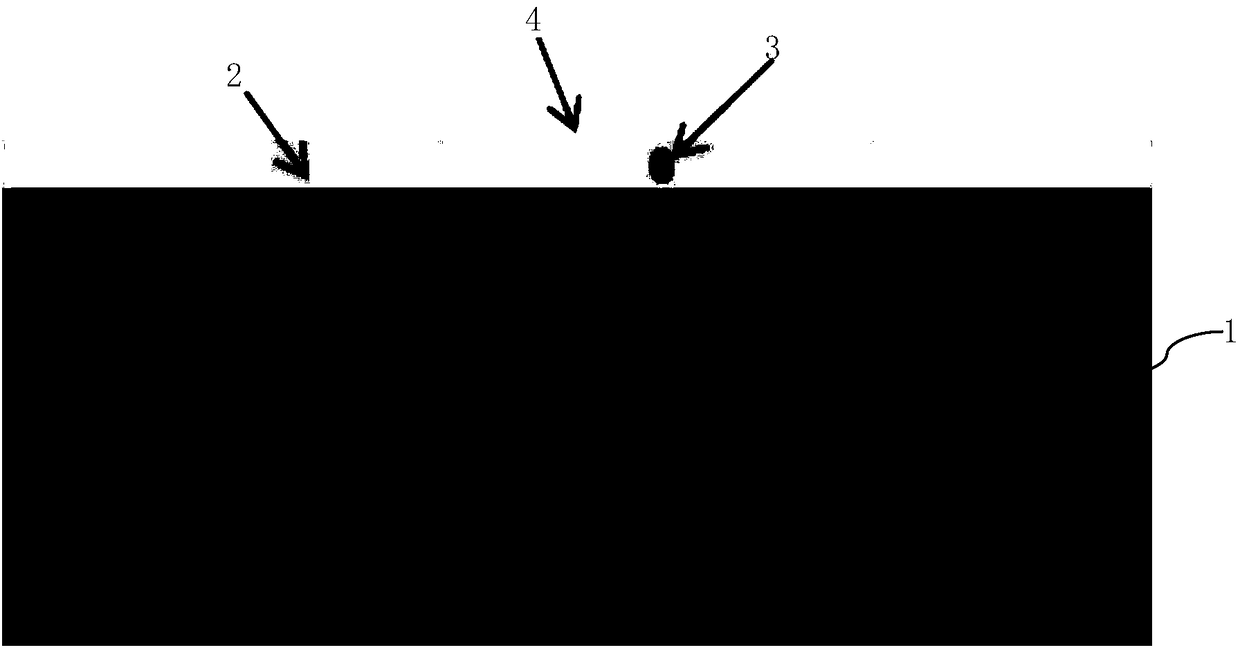
[0031] Step one, as Figure 3A As shown, a chip that needs to be made into a TEM sample 201 is provided. The device layer 2 of the chip is formed on the surface of the semiconductor substrate 1, and nickel metal silicide is formed on the interface between the device layer 2 and the semiconductor substrate 1. in the selected area. In the method of the embodiment of the present invention, the semiconductor substrate 1 is a single crystal silicon substrate.

[0032] Step two, as Figure 3A As shown, a metal protection layer 4 is formed on the surface of the select...


PUM

PropertyMeasurementUnit
Thicknessaaaaaaaaaa

Abstract

The invention discloses a preparation method of a TEM sample of a nickel metal silicide. The method includes steps of: 1) providing a chip, wherein the nickel metal silicide is formed in selected zones in a device layer and a semiconductor substrate interface of the chip; 2) forming a metal protective layer so as to completely cover a target zone that requires TEM analysis; 3) cutting the TEM sample used for TEM analysis by means of ion beam; 4) turning the chip to a certain degree, and performing ion bombarding to the semiconductor substrate layer of the chip by means of the ion beam to completely amorphize the semiconductor substrate layer. The method can improve the TEM contract imaging difference between the semiconductor substrate layer and the TEM sample, and can form the TEM samplewhich allows clear imaging of the nickel metal silicide in a TEM mode, thereby reducing TEM observation time and reducing observation cost of the sample.

Description

technical field [0001] The invention relates to a method for manufacturing a semiconductor integrated circuit, in particular to a method for preparing a transmission electron microscope (TEM) sample of nickel metal silicide. Background technique [0002] TEM is a very important analytical tool in materials science research. It can perform morphology analysis, structural analysis and composition analysis of samples. It has an extremely wide and increasingly important application in the field of integrated circuit analysis. Focused ion beam (FIB) Sample preparation is the most important TEM sample preparation method in the semiconductor field. [0003] With the improvement of chip technology nodes, nickel silicide, namely nickel metal silicide, is used in integrated circuit manufacturing processes, and the phenomenon of chip failure caused by structural defects of nickel silicide (NiSi) is also increasing. The conventional method of preparing TEM samples by FIB, in order to a...

Claims


Application Information

Patent Timeline
IPC IPC(8): G01N1/28G01N23/04
CPCG01N1/28G01N23/04
Inventor 陈胜陈强史燕萍
Owner SHANGHAI HUALI MICROELECTRONICS CORP
Why Eureka
Try Eureka