

Via anti-pad layout method, device, PCB and via anti-pad manufacturing device
A technology for manufacturing devices and anti-pads, applied in the field of printed circuit boards, can solve problems such as complex design and processing, and achieve the effects of reducing design and processing difficulty, improving design and processing efficiency, and reducing processing costs.
- Summary
- Abstract
- Description
- Claims
- Application Information
AI Technical Summary
Problems solved by technology
Method used
Image

Examples
no. 1 example
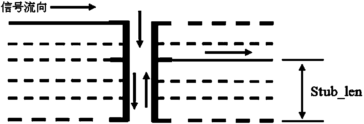
[0048] In the first embodiment of the present invention, a method for arranging via anti-pads, such as Figure 1 ~ Figure 2 shown, including the following specific steps:
[0049] Step S101, the layout device selects the size of the differential signal via anti-pad of the PCB corresponding to the quarter-wavelength resonance frequency of the differential signal via hole of the PCB when it is equal to the set frequency as the anti-pad of the differential signal via hole of the PCB smallest size.
[0050] Wherein, the set frequency is the maximum frequency in the differential mode insertion loss frequency range specified by the high-speed signal transmission protocol.
[0051] High-speed signal transmission protocols include but are not limited to: Institute of Electrical and Electronics Engineers 10G High-speed Backplane System Transmission Protocol (IEEE802.3ap-10GBase-KR), Institute of Electrical and Electronics Engineers 25G High-speed Backplane System KR4), Optical Networki...
no. 2 example
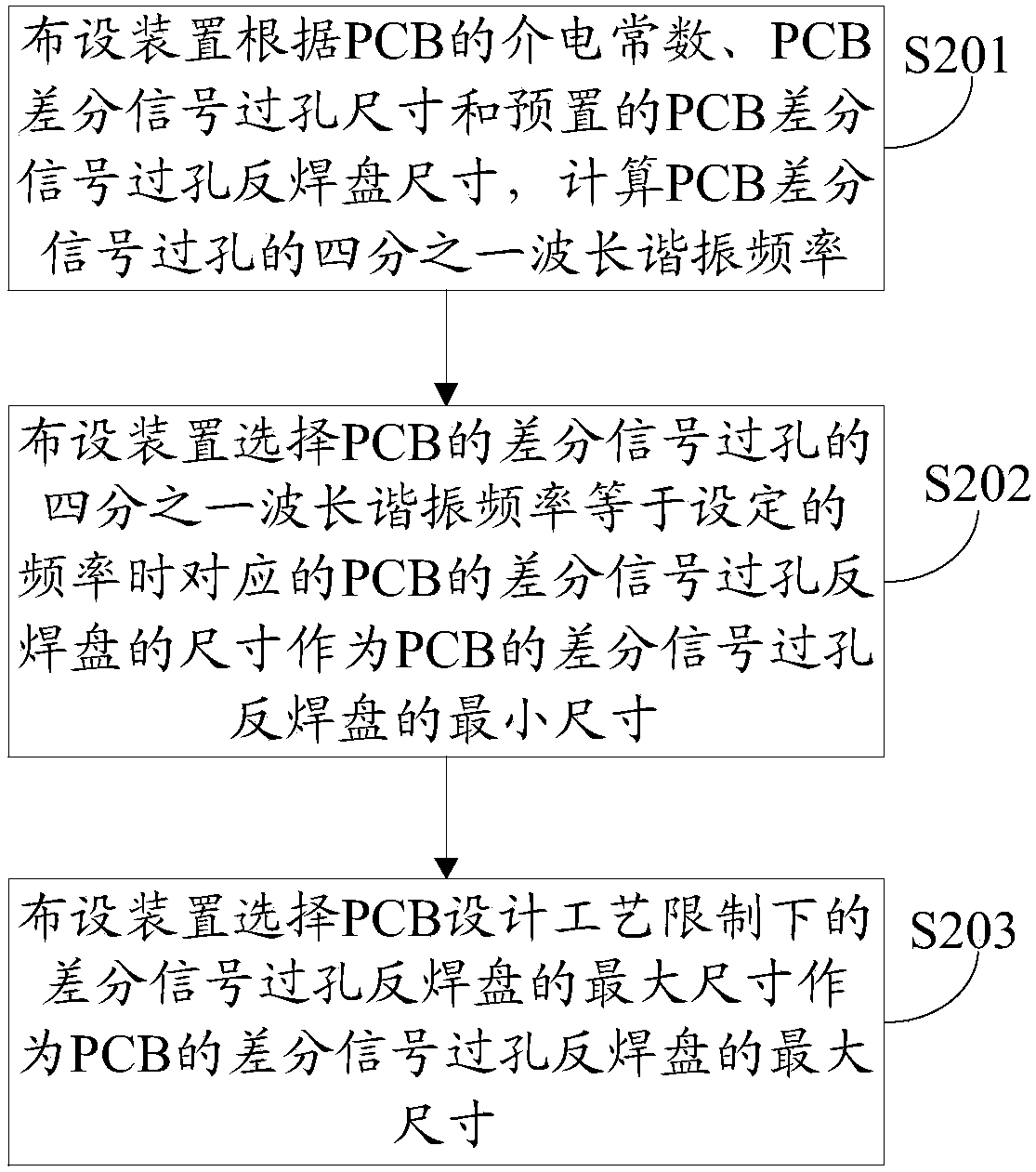
[0084] In the second embodiment of the present invention, a method for arranging via anti-pads, such as image 3 shown, including the following specific steps:
[0085] Step S201, the layout device calculates the quarter-wavelength resonant frequency of the PCB differential signal via hole according to the dielectric constant of the PCB, the size of the PCB differential signal via hole and the preset size of the anti-pad of the PCB differential signal via hole.
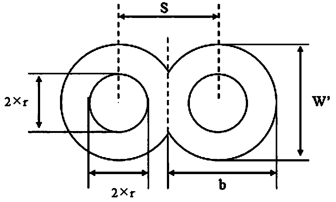
[0086] Among them, the anti-pad of the differential signal via is a circle, a rectangle, or a playground shape composed of a rectangle and two semicircles;
[0087] Differential signal vias are round or rectangular.
[0088] The number of stacked layers of the PCB is greater than or equal to 4 layers.
[0089] In the case that the differential signal via hole anti-pad is circular, and the differential signal via hole is circular, according to the dielectric constant of the PCB, the size of the differential signal vi...
no. 3 example
[0137] In the third embodiment of the present invention, a device for arranging via anti-pads includes the following components:
[0138] The allocation module 200 is used to select the size of the corresponding PCB differential signal via anti-pad when the quarter-wavelength resonant frequency of the differential signal via hole of the PCB is equal to the set frequency as the differential signal via anti-pad of the PCB minimum size of .
[0139] Wherein, the set frequency is the maximum frequency in the differential mode insertion loss frequency range specified by the high-speed signal transmission protocol.
[0140] High-speed signal transmission protocols include but are not limited to: Institute of Electrical and Electronics Engineers 10G High-speed Backplane System Transmission Protocol (IEEE802.3ap-10GBase-KR), Institute of Electrical and Electronics Engineers 25G High-speed Backplane System KR4), Optical Networking Forum General Electric Transceiver Protocol 25G High S...
PUM
| Property | Measurement | Unit |
|---|---|---|
| Dielectric constant | aaaaa | aaaaa |
Abstract
Description
Claims
Application Information