Flexible display panel and flexible display device

A flexible display and panel technology, applied in photovoltaic power generation, electrical components, electrical solid devices and other directions, can solve the problems of complex flexible display panel process, and achieve the effect of simplifying the structure, reducing the resistance value, and reducing the process cost.

Inactive Publication Date: 2018-06-08
SUZHOU QUINGYUE OPTOELECTRONICS TECH CO LTD
10 Cites 3 Cited by

AI-Extracted Technical Summary

Problems solved by technology

[0004] However, the addition of auxiliary electrodes will ine...

Method used

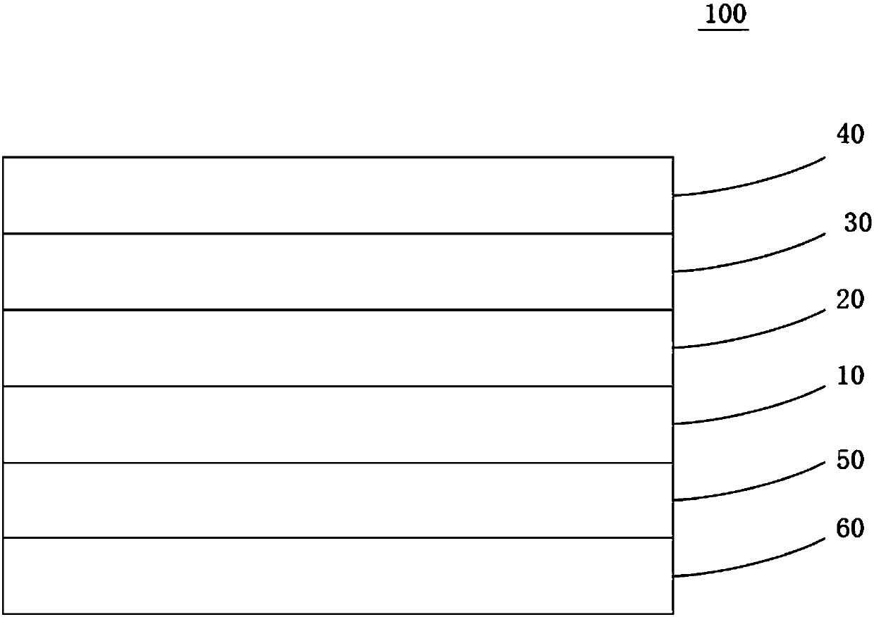
[0025] In one embodiment of the present invention, a flexible display panel 100 is provided, the anode layer 10 of the flexible display panel 100 is a transparent conductive layer, which has the property of light transmission and the function of conduction. The requirement that the anode layer 10 can transmit visible light is to meet the requirement that the light of the organic material in the flexible display panel 100 needs to pass through the anode layer 10 to exit. Specifically, the anode layer 10 is a metal layer, a nano-carbon layer, a graphene layer, or a composite layer of two or mo...

Abstract

The invention discloses a flexible display panel and a flexible display device, which relate to the technical field of flexible display panels. The flexible display panel comprises an anode layer, theanode layer is a transparent conductive layer, the transparent conductive layer is a metal layer, a nano carbon layer, a graphene layer, or a composite layer of two or more of the layers, wherein work function of a metal material in the metal layer is more than 4.5ev. According to the flexible display panel provided by the invention, a conventional ITO is not used for the anode layer, but the metal layer, the nano carbon layer or the graphene layer with a relatively low resistance value is used as the anode layer. The structure is free from being provided with an auxiliary electrode to reducethe resistance value of an anode, is beneficial for simplification of the structure of the flexible display panel and can reduce process cost.

Application Domain

Solid-state devicesSemiconductor/solid-state device manufacturing +2

Technology Topic

Auxiliary electrodeWork function +8

Image

  • Flexible display panel and flexible display device

Examples

  • Experimental program(1)

Example Embodiment

[0024] In order to make the objectives, technical solutions and advantages of the present invention clearer, the technical solutions of the present invention will be described clearly and completely in conjunction with specific embodiments of the present invention and the corresponding drawings. Obviously, the described embodiments are only a part of the embodiments of the present invention, rather than all the embodiments. Based on the embodiments of the present invention, all other embodiments obtained by those of ordinary skill in the art without creative work shall fall within the protection scope of the present invention.
[0025] In an embodiment of the present invention, a flexible display panel 100 is provided. The anode layer 10 of the flexible display panel 100 is a transparent conductive layer, which has light-transmitting properties and conductive functions. The anode layer 10 is required to transmit visible light in order to meet the requirement that the light of the organic material in the flexible display panel 100 needs to pass through the anode layer 10 to exit. Specifically, the anode layer 10 is a metal layer, a nanocarbon layer, a graphene layer, or a composite layer of two or more of them. The work function of the metal material in the metal layer selected in the present invention is above 4.5 eV. The metal layer is formed by selecting a metal material with a relatively high work function, which helps to reduce the resistance of the metal layer. However, choosing a metal layer, a nano carbon layer or a graphene layer with a lower resistance value as the anode layer does not require an auxiliary electrode to reduce the resistance of the anode, which is also beneficial to simplify the structure of the flexible display panel and reduce the process cost.
[0026] In the embodiment in which a metal layer is used as the anode layer 10, the work function of the metal material in the metal layer is preferably above 4.8ev, more preferably above 5ev, preferably in the range of 5-6ev. The metal materials that can be selected include but are not limited to At least one of nickel, gold or platinum. Among them, the work function values ​​of gold and platinum both exceed 5.1 eV, and the work function value of nickel is 5.15 eV. A higher work function value can facilitate hole injection and improve the luminous efficiency of the flexible display panel 100.
[0027] The thickness of the anode layer 10 should be suitable for visible light transmission and have a reasonable bending radius. In the embodiment of the present invention, when the anode layer 10 is a metal layer, in order for visible light to penetrate the anode layer 10, the thickness of the metal layer should be More preferably in Below, for example in The smaller the thickness, the higher the light transmittance of the metal layer, and the more favorable the light emission of the organic layer 20 is. Therefore, the thickness of the metal layer can be or
[0028] It should be noted that the above thickness unit Is a unit of length, which is equivalent to one tenth of a nanometer, that is Equal to 15 nanometers.
[0029] In the embodiment where a carbon nano layer is used as the anode layer 10, the carbon material in the carbon nano layer is preferably in the form of carbon nanotubes or carbon fibers; this carbon nano layer can conduct electricity, and the work function of the carbon nanotubes is 4.8 eV, It meets the selection standard of OLED anode material; and this carbon nano layer can be made into a transparent state for light to penetrate, so as to meet the requirements of the present invention for the anode layer. In this embodiment, the nano-carbon layer may be a material layer containing only nano-carbon materials, or a composite material layer that includes both nano-carbon materials and other materials and can meet the foregoing requirements for the anode layer 10.
[0030] In the embodiment where a graphene layer is used as the anode layer 10, the graphene layer may be a material layer containing only graphene, or it may be a composite material that includes both graphene and other materials and can meet the foregoing requirements for the anode layer 10 Floor.
[0031] In addition, the smaller the thickness of the anode layer 10 is, the smaller the bending radius it can bear, which can achieve a larger angle of bending. In the present invention, the bending radius of the anode layer 10 may be 20 mm or less.
[0032] In the embodiment of the present invention, the anode layer 10 is formed of one of a metal layer, a nano carbon layer or a graphene layer. Of course, in some special embodiments, the anode layer 10 may be formed by a mixture of two of a metal layer, a nano carbon layer, or a graphene layer.
[0033] The flexible display panel 100 further includes a cathode layer 30 and an organic layer 20, and the organic layer 20 is sandwiched between the anode layer 10 and the cathode layer 30. When a metal layer is selected for the cathode layer, the work function of the metal material in the cathode layer 30 is smaller than the work function of the metal material in the metal layer suitable as the anode layer 10. In one embodiment, the metal material in the cathode layer 30 may be silver, Aluminum, lithium or magnesium.
[0034] The flexible display panel 100 further includes a water blocking layer, which is made of airtight material to protect the anode layer 10, the cathode layer 30, and the organic layer 20 in the flexible display panel 100. Specifically, the water blocking layer includes a first water blocking layer 40 and a second water blocking layer 50. The first water blocking layer 40 is disposed on the cathode layer 30 and opposite to the organic layer 20. The second water blocking layer 50 is disposed under the cathode layer 30 and opposite to the organic layer 20. The applicable airtight material can be inorganic or a combination of organic and inorganic, and the inorganic can be selected from SiO 2 , Si 3 N 4 And Al 2 O 3 At least one of the organic substances may be polymerized carbon oxide compounds.
[0035] The flexible display panel 100 further includes a flexible substrate 60, and the second water blocking layer 50 is disposed on the flexible substrate 60.
[0036] In the embodiment of the present invention, the flexible display panel 100 further includes an encapsulation layer disposed on the first water blocking layer 40.
[0037] Such as figure 1 As shown, in a relatively specific embodiment of the present invention, the flexible display panel 100 includes from top to bottom: a first water blocking layer 40, a cathode layer 30, an organic layer 20, an anode layer 10, and a second water blocking layer. Layer 50 and flexible substrate 60. The light from the organic layer 20 passes through the anode layer 10 and exits from the flexible substrate 60.
[0038] In another embodiment of the present invention, a flexible display device is also provided, and the flexible display device has the above-mentioned flexible display panel 100.
[0039] The specific examples described above further describe the purpose, technical solutions and beneficial effects of the present invention in further detail. It should be understood that the above are only specific embodiments of the present invention and are not intended to limit the present invention. Within the spirit and principle of the present invention, any modification, equivalent replacement, improvement, etc., shall be included in the protection scope of the present invention.

PUM

PropertyMeasurementUnit
Work function>= 4.5eV
Work function>= 4.8eV
Work function>= 5.0eV

Description & Claims & Application Information

We can also present the details of the Description, Claims and Application information to help users get a comprehensive understanding of the technical details of the patent, such as background art, summary of invention, brief description of drawings, description of embodiments, and other original content. On the other hand, users can also determine the specific scope of protection of the technology through the list of claims; as well as understand the changes in the life cycle of the technology with the presentation of the patent timeline. Login to view more.

Similar technology patents

Thin film transistor, preparation method thereof, array substrate and display device

PendingCN107910375Alower resistanceImprove light stability
Owner:BOE TECH GRP CO LTD

Classification and recommendation of technical efficacy words

  • Simple structure
  • Lower resistance

Laser diode and manufacturing method thereof

ActiveUS20050127383A1lower resistancelight increase
Owner:LUMENTUM JAPAN INC

Top grid self-alignment thin-film transistor with source/drain areas raised and manufacturing method thereof

ActiveCN103346093Alower resistanceavoid parasitic effects
Owner:PEKING UNIV SHENZHEN GRADUATE SCHOOL

Electrical heating device

Owner:HTTP HYPOTHERMIA THERAPY

Electrolyte and lithium ion battery

Owner:湛江市金灿灿科技有限公司
Why Eureka
Try Eureka