
Method for relieving metal residues at side step of polycrystalline silicon structure

A metal residue, polysilicon technology, applied in electrical components, semiconductor/solid-state device manufacturing, circuits, etc., can solve the problems of tungsten residue and difficult to completely remove, and achieve the effect of eliminating metal residue and reducing the vertical structure at the step.

Active Publication Date: 2018-06-29
SHANGHAI HUAHONG GRACE SEMICON MFG CORP
View PDF5 Cites 3 Cited by
  • Summary
  • Abstract
  • Description
  • Claims
  • Application Information

AI Technical Summary

Problems solved by technology

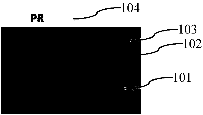
but by Figure 1D It can be seen that, since the BPSG at the side steps of the polysilicon gate 1031 has a steep structure, the tungsten 107 at the side steps of the polysilicon gate 1031 is not easy to be completely removed, and tungsten residues are likely to occur.

Method used


Image

  • Method for relieving metal residues at side step of polycrystalline silicon structure
  • Method for relieving metal residues at side step of polycrystalline silicon structure
  • Method for relieving metal residues at side step of polycrystalline silicon structure

Examples


Embodiment Construction

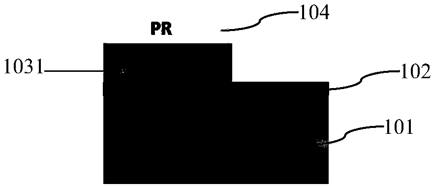
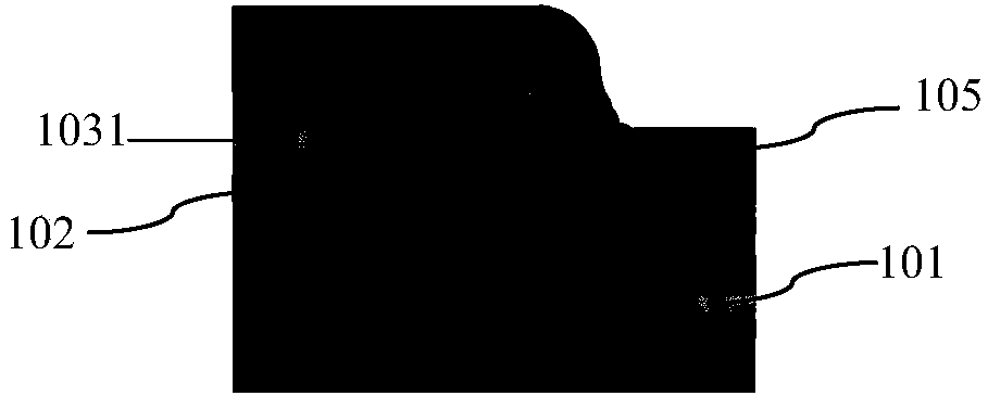
[0040] Such as figure 2 As shown, it is a flow chart of the method for improving the metal residue on the side of the polysilicon step in the embodiment of the present invention; as Figure 3A to Figure 3E As shown, it is a schematic diagram of the device structure in each step of the method of the embodiment of the present invention. The method for improving the metal residue on the side of the polysilicon step in the embodiment of the present invention includes the following steps:

[0041] Step 1, such as Figure 3A As shown, a polysilicon layer 3 is formed, and a photoresist pattern 4 is formed by a photolithography process to define a formation area of ​​a polysilicon structure 31 . Photoresist pattern 4 in Figure 3A Also marked with PR.

[0042] In the method of the embodiment of the present invention, the polysilicon layer 3 in step 1 is formed on the surface of a semiconductor substrate such as a silicon substrate 1 . A gate oxide layer 2 is formed on the surface...


PUM


Abstract

The invention discloses a method for relieving metal residues at a side step of a polycrystalline silicon structure. The method comprises the following steps of forming a polycrystalline silicon layer, and performing photoetching to define a forming area of a polycrystalline silicon structure; etching for the first time in an isotropy way; etching for the second time in the isotropy way, wherein avertical structure is formed at the side step of the polycrystalline silicon structure, and the top part of the vertical structure is of a circular arc structure which is formed during first-time etching; depositing an interlayer film which is formed by stacking common-pressure silicon oxide and boron-phosphorosilicate glass, wherein the thickness of the interlayer film is greater than or equal to the thickness of the vertical structure at the side step of the polycrystalline silicon structure; annealing and refluxing, wherein the boron-phosphorosilicate glass after refluxing forms a completely inclined structure at the side step of the polycrystalline silicon structure; forming an opening in contact with a hole; forming a metal layer, and performing metal etching. The method has the advantage that the boron-phosphorosilicate glass is of the completely inclined structure at the side step of the polycrystalline silicon structure, so as to eliminate the metal residues at the side step of the polycrystalline silicon layer.

Description

technical field [0001] The invention relates to a method for manufacturing a semiconductor integrated circuit, in particular to a method for improving metal residues on the side surfaces of polysilicon steps. Background technique [0002] In semiconductor integrated circuits, electrostatic discharge (ESD) will cause damage to devices, so ESD protection circuits need to be installed at the input and output ends of integrated circuits for electrostatic protection. Existing devices for ESD protection circuits include laterally diffused metal oxide semiconductors ( LDMOS). The LDMOS device includes a gate structure composed of a polysilicon layer, that is, a polysilicon gate. The polysilicon gate will form a stepped structure on the surface of the device. In the subsequent process of the polysilicon gate, an interlayer film and a contact hole will be formed. The contact hole includes the interlayer film in the contact area. Remove the step of forming the opening and the step of...

Claims


Application Information

Patent Timeline
Patent Type & Authority Applications(China)
IPC IPC(8): H01L21/02H01L21/71
CPCH01L21/02068H01L21/71
Inventor 张辉陈正嵘周颖
Owner SHANGHAI HUAHONG GRACE SEMICON MFG CORP
Learn More