A crystal back thinning method and used circular jig
A wafer and circular technology, applied in the manufacture of electrical components, circuits, semiconductors/solid-state devices, etc., can solve the problems of difficult fine control of the grinding area, prone to damage, wafer breakage, etc., to simplify the wafer thinning process , to avoid the effect of fragmentation
- Summary
- Abstract
- Description
- Claims
- Application Information
AI Technical Summary
Problems solved by technology
Method used
Image

Examples
Embodiment Construction
[0026] The present invention will be described in further detail below through specific examples.
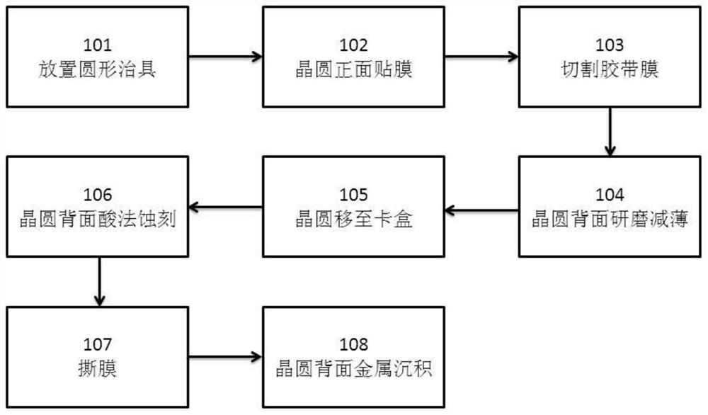
[0027] exist figure 1 Shown in is the specific embodiment of the crystal back thinning method disclosed in the present invention, in this embodiment:
[0028] In step 101, a circular jig is placed on the back of the wafer, so that the wafer is completely embedded in the center of the circular jig and attached to the inner edge of the circular jig;
[0029] Then proceed to step 102. In step 102, use a glue applicator to attach a layer of tape film on the front of the wafer, and make the tape film attached to the front of the wafer protrude from the outer edge of the wafer and the circular jig. Acidic or alkaline solution reacts and the tape film is larger than the wafer area;
[0030] Then proceed to step 103, in step 103, cut the tape film attached to the front of the wafer along the outer edge of the circular jig, so that the tape film protrudes from the wafer by 1-2mm;
[0...
PUM
 Abstract
Description
Claims
Application Information
 - Generate Ideas
- Intellectual Property
- Life Sciences
- Materials
- Tech Scout
- Unparalleled Data Quality
- Higher Quality Content
- 60% Fewer Hallucinations
Browse by: Latest US Patents, China's latest patents, Technical Efficacy Thesaurus, Application Domain, Technology Topic, Popular Technical Reports.
© 2025 PatSnap. All rights reserved.Legal|Privacy policy|Modern Slavery Act Transparency Statement|Sitemap|About US| Contact US: help@patsnap.com