Array substrate, manufacturing method, display panel and display device

A technology of an array substrate and a manufacturing method, applied in the fields of display panels and display devices, manufacturing methods and array substrates, can solve the problems of process incompatibility, difficulty in reducing the number of masks, multi-mask processes, etc., so as to solve the problem of process incompatibility , the effect of reducing the number of masks

Active Publication Date: 2020-06-30
BOE TECH GRP CO LTD
View PDF8 Cites 0 Cited by
  • Summary
  • Abstract
  • Description
  • Claims
  • Application Information

AI Technical Summary

Problems solved by technology

However, due to the need to combine the two processes of LTPS and Oxide, the process will inevitably become complicated, that is, more Mask processes need to be used
In order to reduce production costs, it is necessary to reduce the number of Masks in the LTPS+Oxide TFT structure, but due to the possible process incompatibility of LTPS TFT and Oxide TFT processes, it is very difficult to reduce the number of Masks

Method used


Image

  • Array substrate, manufacturing method, display panel and display device
  • Array substrate, manufacturing method, display panel and display device
  • Array substrate, manufacturing method, display panel and display device

Examples


Embodiment Construction

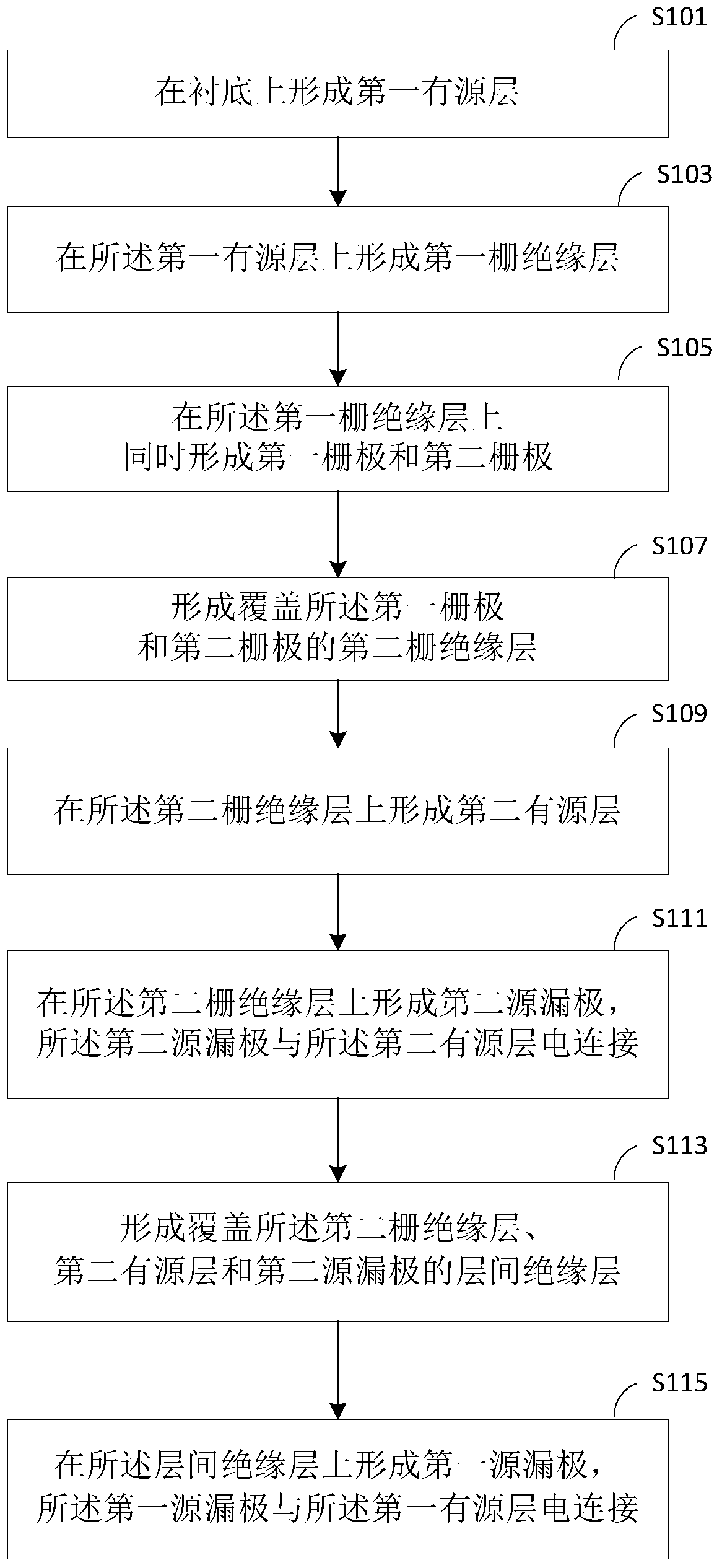
[0042] In order to illustrate the present invention more clearly, the present invention will be further described below in conjunction with preferred embodiments and accompanying drawings. Similar parts in the figures are denoted by the same reference numerals. Those skilled in the art should understand that the content specifically described below is illustrative rather than restrictive, and should not limit the protection scope of the present invention.

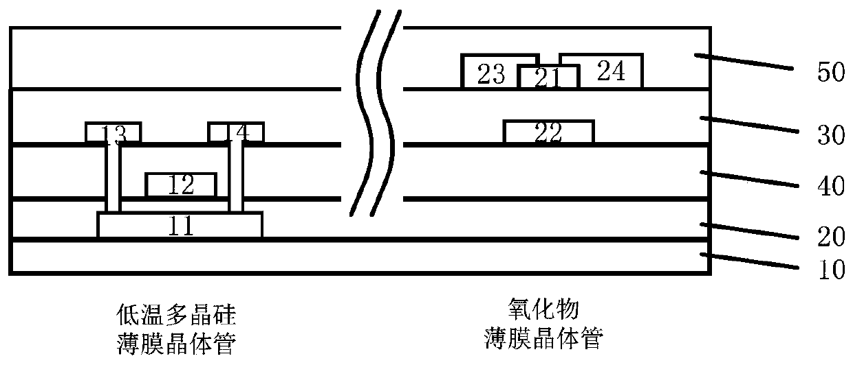
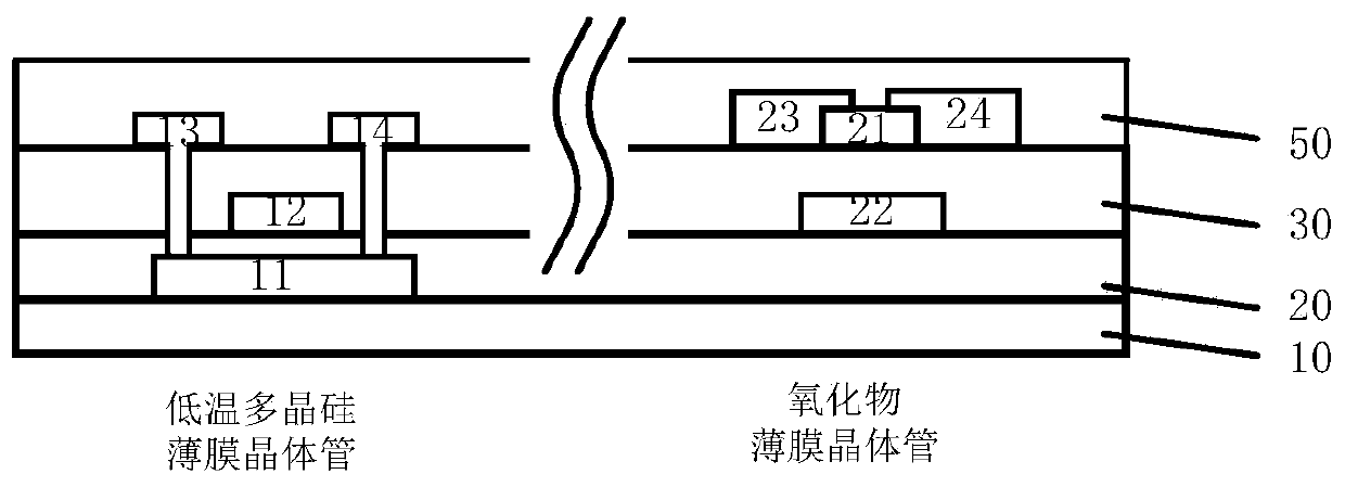
[0043] At present, the existing process that combines the structure of low-temperature polysilicon thin film transistor and oxide thin film transistor is based on the production of LTPS TFT, adding 4 Oxide TFT mask (Mask) processes to form the LTPS+Oxide TFT structure, that is, oxidation Thin film transistor gate insulating layer mask, active layer mask, source and drain mask and passivation layer mask.

[0044] like figure 1 As shown, the left side is the structure of low temperature polysilicon thin film transistor (LTP...


PUM


Abstract

The invention discloses an array substrate, comprising two kinds of thin film transistors, specifically comprising a first active layer formed on the substrate; a first gate insulating layer covering the first active layer; and a first gate insulating layer formed on the first active layer. A first gate and a second gate arranged in the same layer on a gate insulating layer; a second gate insulating layer covering the first gate and the second gate; a first gate formed on the second insulating layer Two active layers and a second source and drain, the second source and drain are electrically connected to the second active layer; an interlayer insulating layer covering the second active layer and the second source and drain; forming The first source and drain on the interlayer insulating layer, the first source and drain are electrically connected to the first active layer. The array substrate, manufacturing method and display device provided in this embodiment can reduce the number of masks in the process of manufacturing two kinds of thin film transistors, and solve the problem of process incompatibility.

Description

technical field [0001] The present invention relates to the field of display technology, in particular to an array substrate, a manufacturing method, a display panel and a display device. Background technique [0002] In recent years, low-temperature polysilicon thin-film transistors (LTPS TFT) and oxide thin-film transistors (Oxide TFT) have attracted much attention in the display industry, and each has its own advantages. LTPS TFT has the advantages of high mobility and fast charging, and Oxide TFT has the advantage of low leakage current. If the advantages of these two materials can be combined, the user experience of display products will be greatly improved. However, due to the need to combine the two processes of LTPS and Oxide, the process will inevitably become complicated, that is, more Mask processes need to be used. In order to reduce production costs, it is necessary to reduce the number of Masks in the LTPS+Oxide TFT structure, but due to the possible process ...

Claims


Application Information

Patent Timeline
Patent Type & Authority Patents(China)
IPC IPC(8): H01L27/12H01L21/77G02F1/1362
CPCG02F1/136277H01L27/1214H01L27/1259H01L2021/775G02F1/1368G02F2202/104H01L27/1225H01L27/1251H01L27/1255G02F1/13685G02F1/133514G09G3/3258H01L29/6675G02F1/133345G02F1/136213H01L29/7869
Inventor 杨维
Owner BOE TECH GRP CO LTD
Why Eureka
Try Eureka