Semiconductor homogeneous substrate and preparation method thereof, preparation method of homoepitaxial layer

A homogenous substrate, homoepitaxy technology, applied in semiconductor/solid-state device manufacturing, semiconductor device, final product manufacturing, etc., can solve the problem of unfavorable lightweight, flexible device development, thermal conductivity and optical rational design, GaN-based semiconductors lack of homogeneity. Substrate, expensive process and other problems, to achieve the effect of improving photovoltaic conversion efficiency, simple mechanical or chemical etching and peeling transfer, and avoiding complex processes

Active Publication Date: 2019-12-10
SHANGHAI ADVANCED RES INST CHINESE ACADEMY OF SCI
View PDF6 Cites 0 Cited by
  • Summary
  • Abstract
  • Description
  • Claims
  • Application Information

AI Technical Summary

Problems solved by technology

[0007] In view of the above-mentioned shortcomings of the prior art, the object of the present invention is to provide a semiconductor homogeneous substrate and its preparation method, and a preparation method of the homoepitaxial layer, which are used to solve the large amount of material waste in the wafer cutting technology in the prior art. ; GaN-based semiconductors lack homogeneous substrates, and there is a lot of room for improvement in film quality and device performance; GaAs-based epitaxial stacked devices are designed with lattice matching and band-gap matching, and the process cost is expensive; the degree of freedom in the choice of wafer thickness is small, which is not conducive to The development of lightweight and flexible devices and the rational design of related electrical conduction, thermal conduction and optics, etc.

Method used


Image

  • Semiconductor homogeneous substrate and preparation method thereof, preparation method of homoepitaxial layer
  • Semiconductor homogeneous substrate and preparation method thereof, preparation method of homoepitaxial layer
  • Semiconductor homogeneous substrate and preparation method thereof, preparation method of homoepitaxial layer

Examples


Embodiment Construction

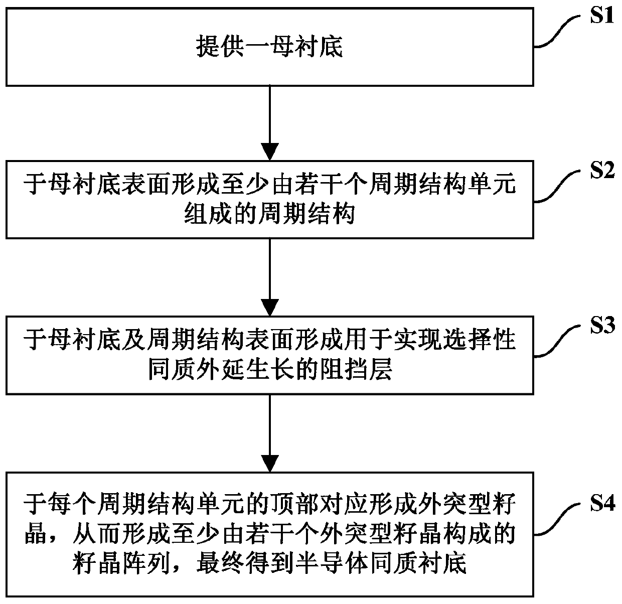
[0068] Embodiments of the present invention are described below through specific examples, and those skilled in the art can easily understand other advantages and effects of the present invention from the content disclosed in this specification. The present invention can also be implemented or applied through other different specific implementation modes, and various modifications or changes can be made to the details in this specification based on different viewpoints and applications without departing from the spirit of the present invention.

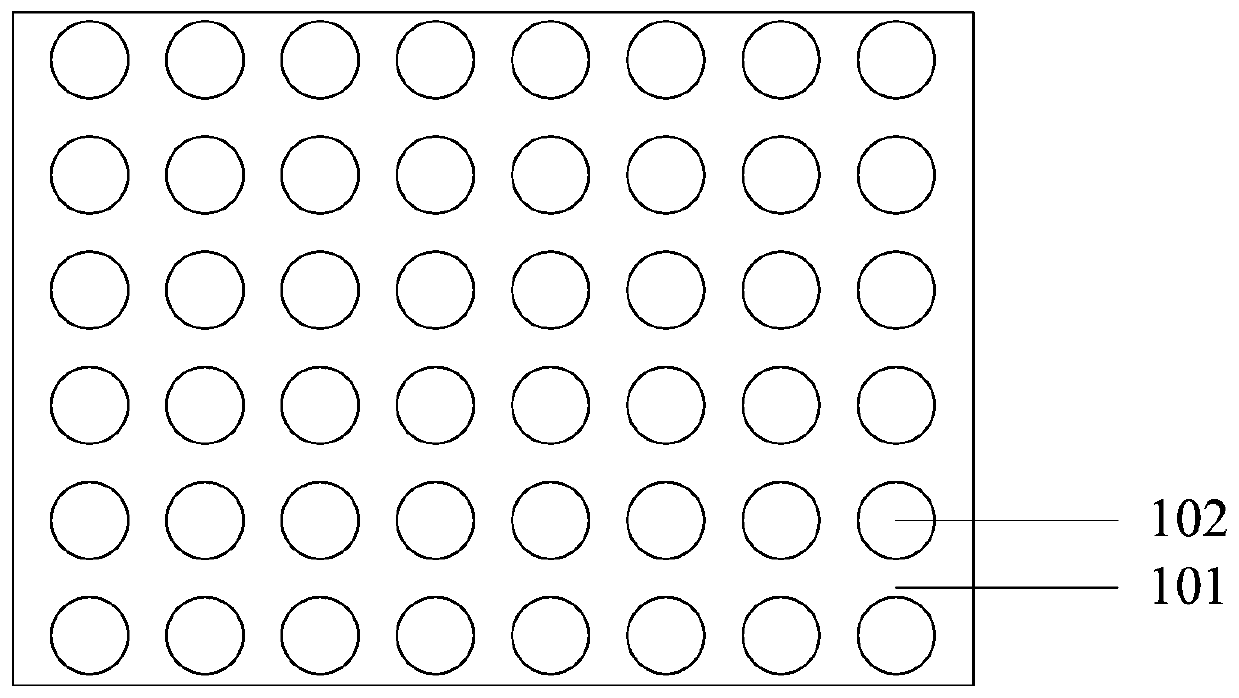
[0069] see Figure 1 to Figure 18 , The first embodiment of the present invention relates to a method for preparing a semiconductor homogeneous substrate. It should be noted that the diagrams provided in this embodiment are only schematically illustrating the basic idea of ​​the present invention, and only the components related to the present invention are shown in the diagrams rather than the number, shape and shape of the component...


PUM

PropertyMeasurementUnit
melting pointaaaaaaaaaa

Abstract

The invention provides a semiconductor homogenous substrate, a preparation method thereof, and a preparation method of a homogeneous epitaxial layer. The preparation method of the semiconductor homogenous substrate at least comprises the following steps that a female substrate is provided, and a period structure composed of period structural units at least is formed in the surface of the female substrate; an epitaxial barrier layer for realizing selective epitaxial growth is formed in the surfaces of the female substrate and the period structure; and epitaxial barrier layers are removed from the tops of the period structural units selectively to form protruded seed crystals correspondingly, a seed crystal array composed of the protruded seed crystals at least is formed, and the semiconductor homogenous substrate is obtained finally. The semiconductor homogenous substrate which can be used repeatedly is used to realize isoepitaxial growth, and the homogenous epitaxial layer which can bepeeled and transferred and is controllable in thickness can be obtained directly. Traditional monocrystalline ingot pulling and slicing processes can be avoided, and a homogenous epitaxial wafer canbe prepared in low cost and high material utilization efficiency.

Description

technical field [0001] The invention relates to the technical field of semiconductor material preparation, in particular to a semiconductor homogeneous substrate, a preparation method thereof, and a preparation method of a homoepitaxial layer. Background technique [0002] Semiconductor technology is the cornerstone of modern high-tech industry. So far, semiconductor materials have roughly experienced three development stages. The first generation is represented by Si and Ge, and the second generation is represented by GaAs (including its In, P and other alloys). , the third generation is represented by GaN (including its In, Al and other alloys), ZnO, and SiC. In current semiconductor technology, single crystal materials are a necessary prerequisite for the realization of high-performance semiconductor devices. [0003] At present, single crystal semiconductor materials are mainly obtained by wire cutting of single crystal ingots to obtain wafers (such as Si, Ge, GaAs, SiC...

Claims


Application Information

Patent Timeline
Patent Type & Authority Patents(China)
IPC IPC(8): H01L31/18H01L21/02H01L31/0304H01L31/0352
CPCH01L21/02389H01L21/0243H01L21/02488H01L31/03044H01L31/035281H01L31/1856H01L31/1896Y02P70/50
Inventor 刘东方张伟曾煌王聪李纪周陈小源鲁林峰
Owner SHANGHAI ADVANCED RES INST CHINESE ACADEMY OF SCI
Why Eureka
Try Eureka