

TFT substrate and manufacturing method thereof
A manufacturing method and substrate technology, which are used in semiconductor/solid-state device manufacturing, optics, instruments, etc., can solve the problems of peeling off the protective layer, difficult to control parameters, poor display of liquid crystal panels, etc., and achieve a small tilt angle and reduce undercutting phenomenon. , show good effect
- Summary
- Abstract
- Description
- Claims
- Application Information
AI Technical Summary
Problems solved by technology
Method used
Image

Examples
Embodiment Construction
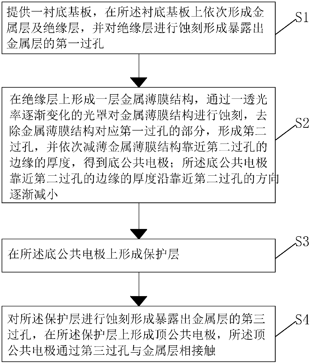
[0031] In order to further illustrate the technical means adopted by the present invention and its effects, the following describes in detail in conjunction with preferred embodiments of the present invention and accompanying drawings.
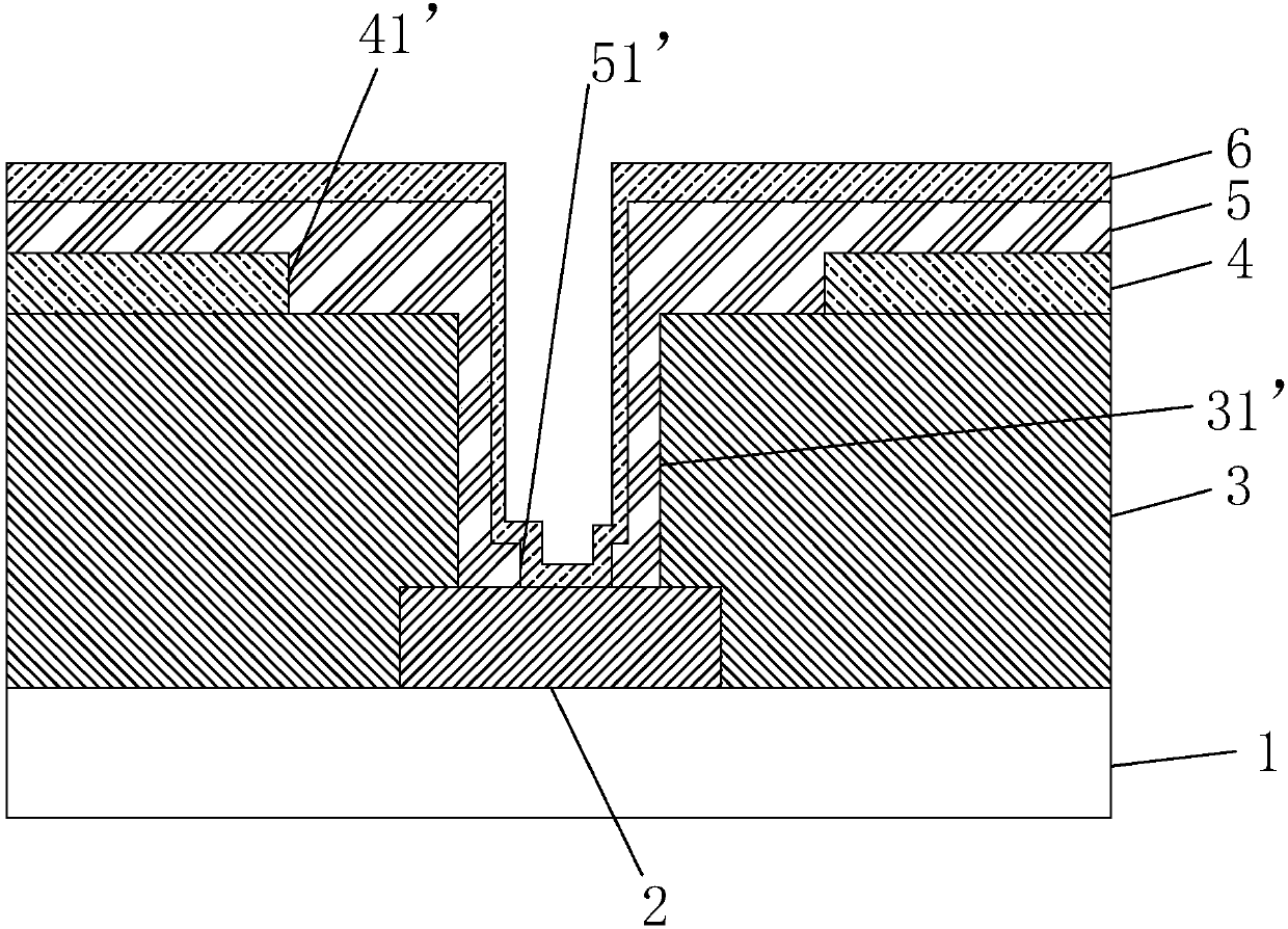
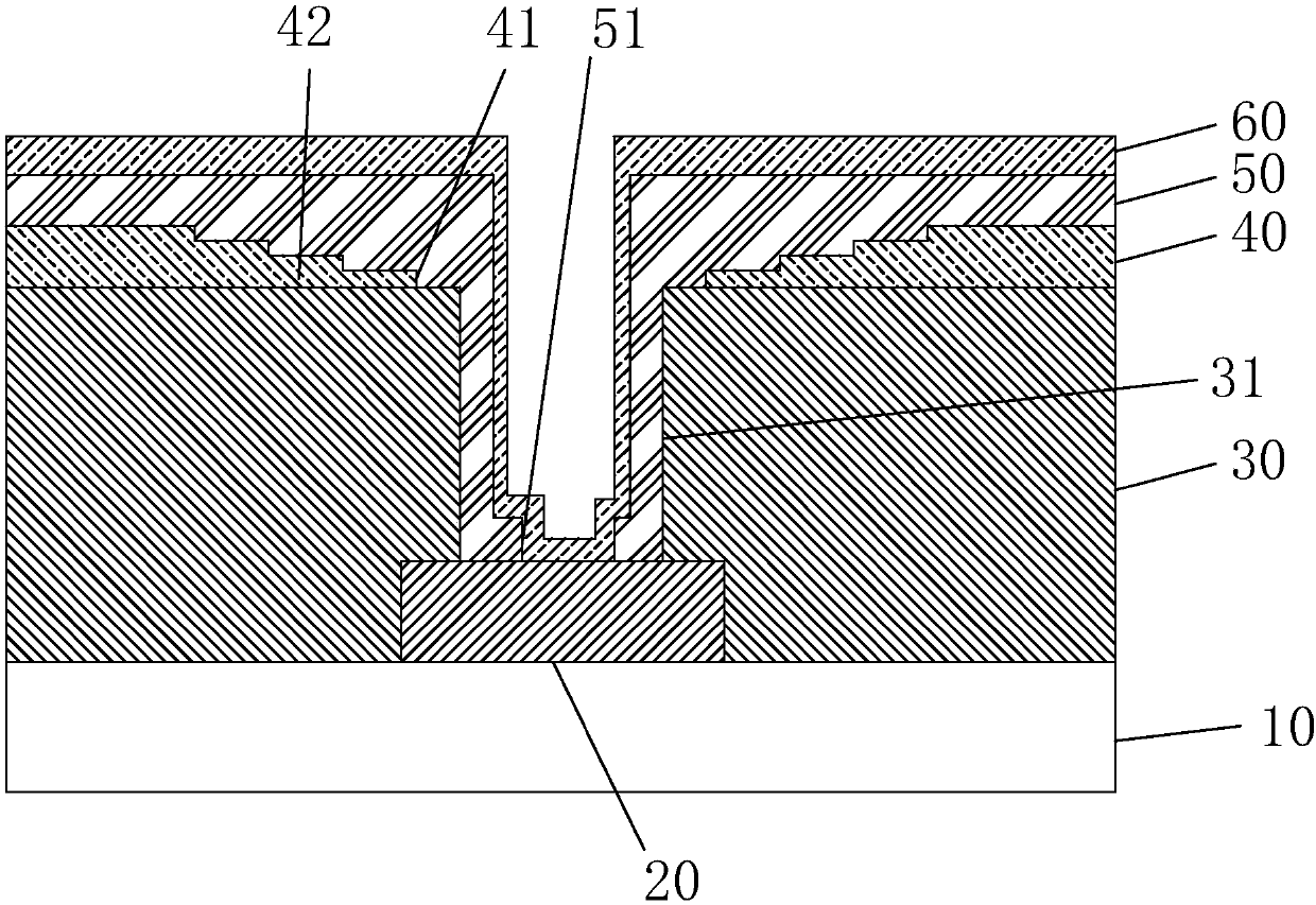
[0032] The drawings in this application are only schematic diagrams. Unless otherwise specified, they do not mean that the actual thickness ratio, flatness, and shape of each film layer are the same as those in the drawings. There are some differences from the schematic diagram, for example, the shape of the hole and the appearance of the combined part of each film layer will be different from the schematic diagram, which can be understood and known by those skilled in the art. The description of the sequence of process steps and the structure of the film layer in this application only indicates the sequence and relative position of the steps and film layers directly related to the technical problems of this application, and does not mean that ...
PUM
| Property | Measurement | Unit |
|---|---|---|
| length | aaaaa | aaaaa |
| transmittivity | aaaaa | aaaaa |
| transmittivity | aaaaa | aaaaa |
Abstract
Description
Claims
Application Information