Thin film transistor, preparation method thereof, array substrate and display device

A technology of thin film transistors and substrate substrates, which is applied in the direction of transistors, semiconductor/solid-state device manufacturing, electric solid-state devices, etc., can solve the problems of cumbersome preparation process and high preparation cost of thin-film transistors, and achieve the goal of reducing the difficulty of process preparation and reducing the preparation cost Effect

Pending Publication Date: 2018-07-06
BOE TECH GRP CO LTD +1
View PDF0 Cites 5 Cited by
  • Summary
  • Abstract
  • Description
  • Claims
  • Application Information

AI Technical Summary

Problems solved by technology

While the driving current and the threshold voltage V of the thin film transistor th Therefore, in practical applications, according to the requirements of different application environments, an additional doping process is performed on the active layer of the thin film transistor to reduce the threshold voltage

Method used


Image

  • Thin film transistor, preparation method thereof, array substrate and display device
  • Thin film transistor, preparation method thereof, array substrate and display device
  • Thin film transistor, preparation method thereof, array substrate and display device

Examples


preparation example Construction

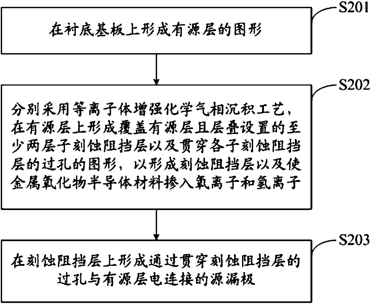
[0043] Based on the same inventive concept, the embodiment of the present invention also provides a method for preparing a thin film transistor, such as figure 2 As shown, the following steps may be included:

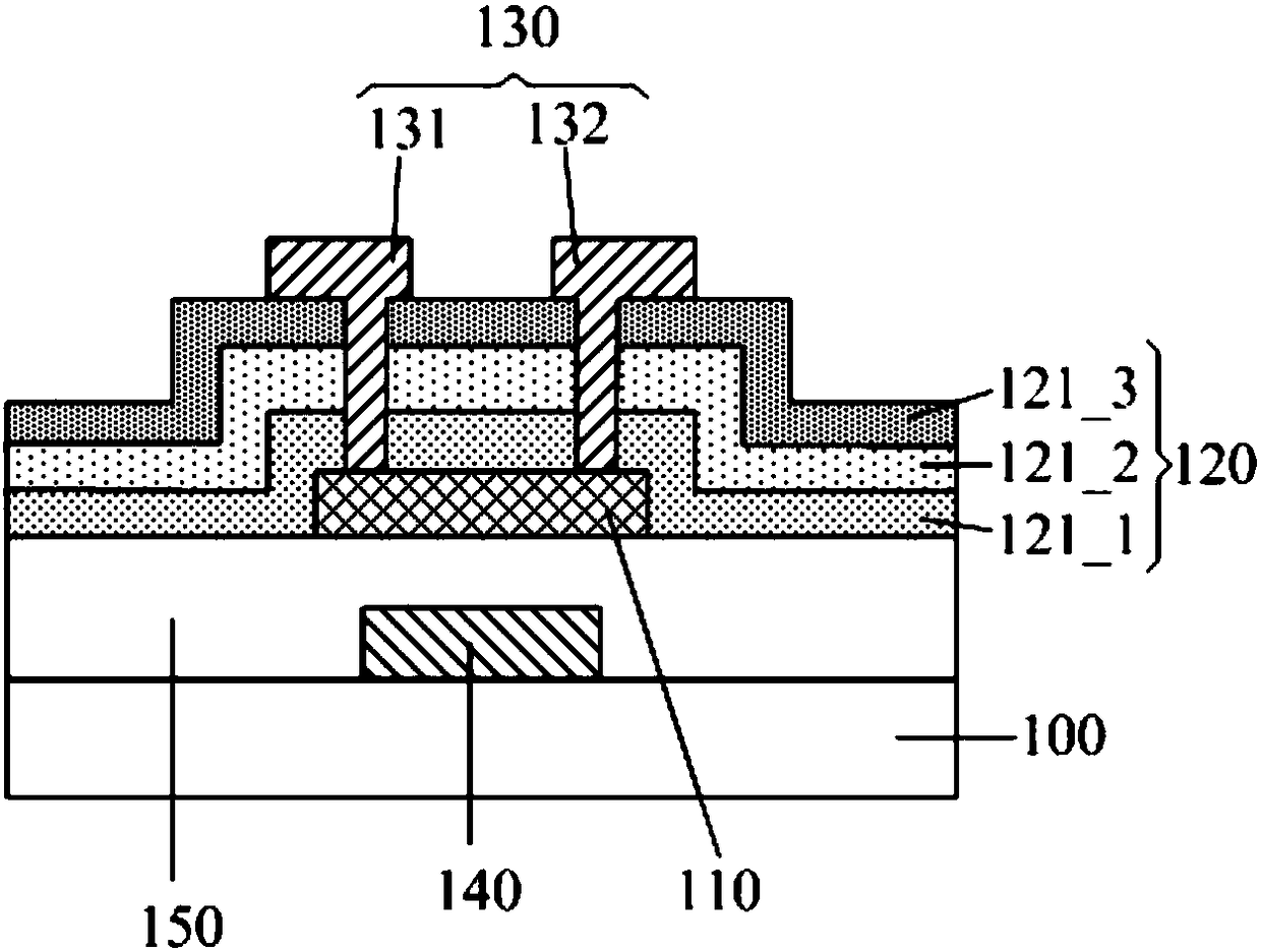
[0044] S201, forming a pattern of an active layer on a base substrate; wherein, the active layer includes a metal oxide semiconductor material;

[0045] S202. Using a plasma-enhanced chemical vapor deposition process to form a pattern of at least two sub-etch stopper layers stacked over the active layer and via holes penetrating through each sub-etch stopper layer on the active layer, so as to form Etching barrier layers and doping metal oxide semiconductor materials with oxygen ions and hydrogen ions;

[0046] S203 , forming source and drain electrodes electrically connected to the active layer through via holes penetrating through the etch barrier layer on the etch barrier layer.

[0047] In the manufacturing method of the thin film transistor provided by the embod...

Embodiment 1

[0070] to prepare figure 1 The structure shown is taken as an example, and the method for preparing a thin film transistor provided in the embodiment of the present invention may include the following steps:

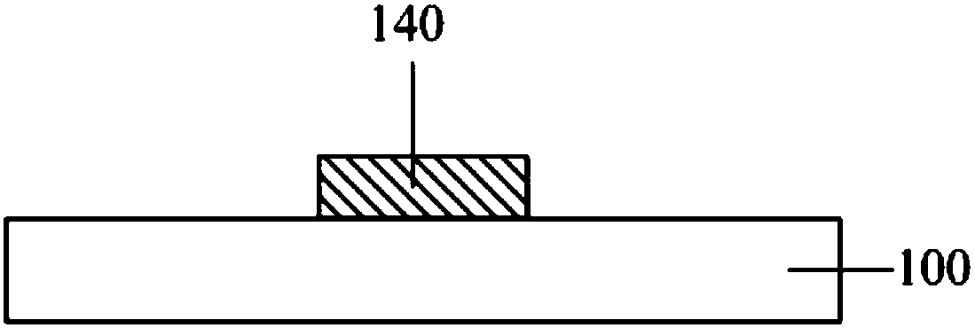
[0071] (1) A gate pattern is formed on a base substrate.

[0072] Specifically, a patterning process is used to form the pattern of the gate 140 on the base substrate 100, such as Figure 3a shown. Wherein, the material of the gate may include Cu.

[0073] (2) Form the pattern of the gate insulating layer 150 covering the gate 140 on the base substrate 100 formed with the gate 140, such as Figure 3b shown.

[0074] Specifically, the gate insulating layer may include two sub-gate insulating layers. Patterns of two layers of sub-gate insulating layers covering the gate are formed on the base substrate on which the gate is formed by using one patterning process respectively.

[0075] (3) A pattern of the active layer is formed on the base substrate on which the gate ...


PUM


Abstract

The invention discloses a thin film transistor, a preparation method thereof, an array substrate and a display device. The threshold voltage of the active layer is regulated by adding oxygen ions andhydrogen ions into the active layer prepared by metal oxide semiconductor materials. When preparing the thin film transistor, each sub-etching barrier layer is obtained by step-by-step deposition using a plasma enhanced chemical vapor deposition process so as to selectively incorporate oxygen ions and hydrogen ions into the metal oxide semiconductor material when each sub-etching barrier layer isdeposited. Thereby regulating the amount of oxygen ions incorporated into the metal oxide semiconductor material and the amount of hydrogen ions incorporated. In this way, the metal oxide semiconductor material can be doped with oxygen ions and hydrogen ions without increasing the additional doping process, so that the preparation difficulty of the process can be reduced and the preparation cost can be reduced.

Description

technical field [0001] The invention relates to the field of display technology, in particular to a thin film transistor, a preparation method thereof, an array substrate and a display device. Background technique [0002] Organic Light Emitting Diode (OLED) displays have the advantages of low energy consumption, low production cost, self-illumination, wide viewing angle, and fast response, and have become one of the research hotspots in the display industry. Since OLED is current-driven, a stable current is needed to control its light emission. Therefore, pixel circuits are generally arranged in the OLED display to drive the OLED to emit light. A general pixel circuit is composed of a plurality of thin film transistors (Thin Film Transistor, TFT) to generate a driving current to drive the OLED to emit light. While the driving current and the threshold voltage V of the thin film transistor th Therefore, in practical applications, according to the requirements of different...

Claims


Application Information

Patent Timeline
IPC IPC(8): H01L27/32H01L29/786H01L21/336
CPCH01L29/66227H01L29/78618H10K59/10H10K59/12
Inventor 彭俊林王东方王玉亮刘增利
Owner BOE TECH GRP CO LTD
Why Eureka
Try Eureka