Vertically-structured LED chip and manufacturing method thereof

An LED chip, vertical structure technology, applied in electrical components, nanotechnology, circuits, etc., can solve the problems of easy falling off of the Ag layer, chip leakage yield, and falling off of the Ag layer, so as to improve the light extraction efficiency, save costs, prevent shedding effect

Active Publication Date: 2018-07-20
HEYUAN CHOICORE PHOTOELECTRIC TECH CO LTD
View PDF3 Cites 5 Cited by
  • Summary
  • Abstract
  • Description
  • Claims
  • Application Information

AI Technical Summary

Problems solved by technology

[0004] In order to overcome the deficiencies of the prior art, one of the purposes of the present invention is to provide a vertical structure LED chip to solve the problem that the Ag layer in the above-mentioned traditional vertical structure LED chip is easy to fall off, so as to cause chip leakage and yield reduction. , can also solve the problem that the Ag layer cannot form a good ohmic contact with the p-GaN layer
[0005] The second object of the present invention is to provide a method for preparing a vertical structure LED chip. The vertical structure LED chip prepared by the preparation method can solve the problems that the above-mentioned Ag layer is easy to fall off, so that the problems such as chip leakage and yield reduction are caused. Solve the problem that the Ag layer cannot form a good ohmic contact with the p-GaN layer

Method used


Image

  • Vertically-structured LED chip and manufacturing method thereof
  • Vertically-structured LED chip and manufacturing method thereof
  • Vertically-structured LED chip and manufacturing method thereof

Examples


Embodiment 31

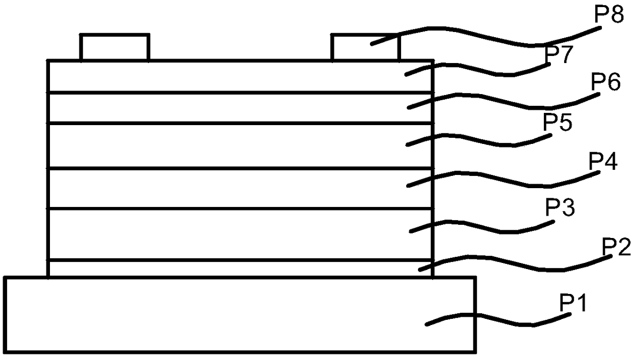
[0063] (1) Growth of LED epitaxial wafers: First, LED epitaxial wafers are epitaxially grown on Si substrates, including n-type doped GaN thin films grown on Si substrates (n-GaN layer P7), grown on n-type doped GaN thin films On the InGaN / GaN quantum well (that is, the InGaN / GaN quantum well layer P6), and the p-type doped GaN film (that is, the p-GaN layer P5) grown on the InGaN / GaN quantum well.

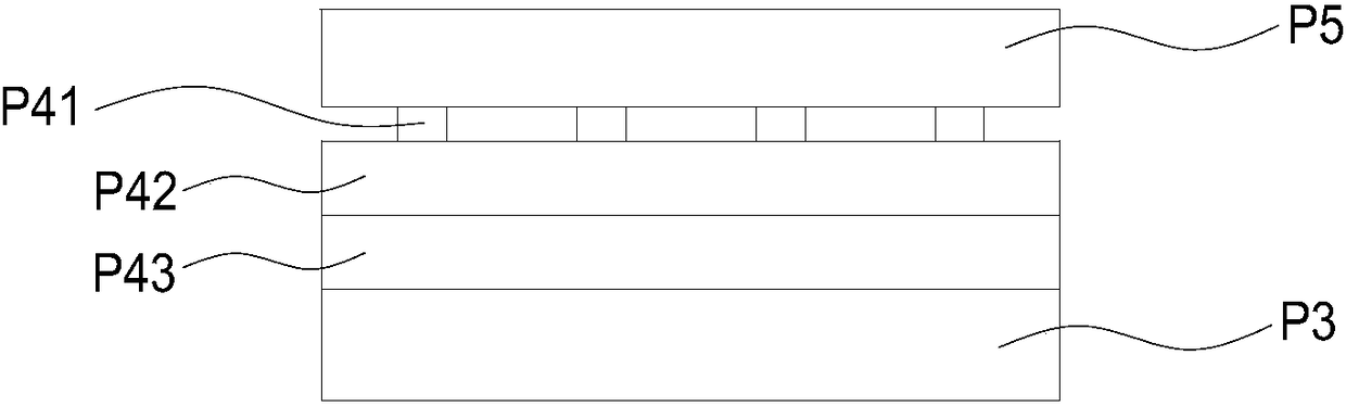
[0064] (2) The first step of growing the nano-point contact layer (metal layer growth): use electron beam evaporation equipment on the surface of the LED epitaxial wafer to evaporate the first contact layer metal Ni / Ag (that is, first evaporate a layer of Ni, and then evaporate Plating a layer of Ag), wherein the thickness of the Ni layer is 3nm; the thickness of the Ag layer is 100nm.

[0065] (3) The second step of growing the nano-point contact layer (metal layer annealing): performing high-temperature annealing on the first contact layer metal Ni / Ag in a rapid annealing furnac...

Embodiment 32

[0077] Example 32 The method for preparing a vertical structure LED chip is generally the same as that of Example 31, the difference lies in:

[0078] (3) The second step of growing nano-point contact layer (metal layer annealing): N 2 with O 2 The ratio of the amount of substances to N 2 :O 2 =20:1, the annealing temperature is 300°C, and the annealing time is 300s.

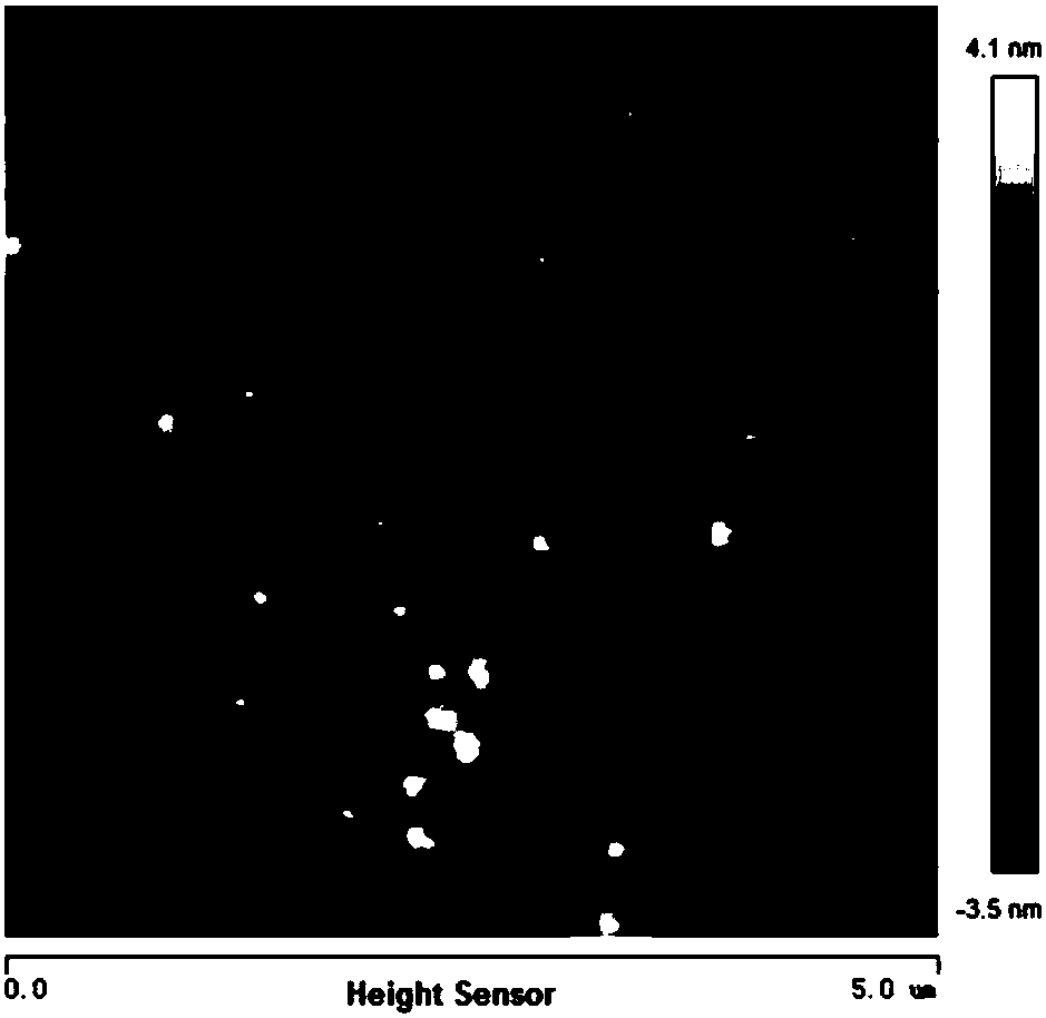
[0079] (4) The third step of growing nano-dot contact layer (wet etching to produce nano-dots): place the alloyed first contact layer prepared in (3) in the prepared acidic corrosion solution aqua regia, soak for 3s and take out .

[0080] (7) The second step of growing mirror layer (metal layer annealing): N 2 with O 2 The ratio of the amount of substances to N 2 :O 2 =1:20, the annealing temperature is 300°C, and the annealing time is 10s.

[0081] (10) Bonding and substrate transfer: the thickness of Sn is 3000nm, and the thickness of Au is 10nm. The LED epitaxial wafer is transferred to the conduct...

Embodiment 33

[0085] (1) Growth of LED epitaxial wafers: First, LED epitaxial wafers are epitaxially grown on Si substrates, including n-type doped GaN thin films grown on Si substrates (n-GaN layer P7), grown on n-type doped GaN thin films On the InGaN / GaN quantum well (that is, the InGaN / GaN quantum well layer P6), and the p-type doped GaN film (that is, the p-GaN layer P5) grown on the InGaN / GaN quantum well.

[0086] (2) The first step of growing the nano-point contact layer (metal layer growth): use thermal evaporation equipment on the surface of the LED epitaxial wafer to evaporate the first contact layer metal Pd / Ag (that is, first evaporate a layer of Pd, and then evaporate Plating a layer of Ag), wherein, the thickness of the Pd layer is 1.5nm; the thickness of the Ag layer is 150nm.

[0087] (3) The second step of growing the nano-point contact layer (metal layer annealing): performing high-temperature annealing on the first contact layer metal Pd / Ag in a rapid annealing furnace t...


PUM


Abstract

The invention discloses a vertically-structured LED chip, which includes a substrate layer and a bonding layer arranged on the substrate layer. The bonding layer is provided with a first protective layer and an X-dots/Ag/Y reflector layer arranged thereon, the X-dots/Ag/Y reflector layer is provided with a p-GaN layer and an InGaN/GaN quantum well layer arranged thereon, and the InGaN/GaN quantumwell layer is provided with an n-GaN layer and n electrode layer arranged thereon. The invention also discloses a manufacturing method of the vertically-structured LED chip. Good adhesion between thereflector layer and the conductive substrate of the vertically-structured LED chip prevents the reflector layer from shedding during a subsequent manufacturing process and also guarantees good ohmic contact between the p-GaN layer and the Ag layer.

Description

technical field [0001] The invention relates to the technical field of LEDs, in particular to a vertical structure LED chip and a preparation method of the vertical structure LED chip. Background technique [0002] With the gradual application of LEDs in the field of lighting, the market has higher and higher requirements for the light efficiency of white LEDs. GaN-based vertical structure LEDs have single-sided light output, good heat dissipation capability, and can withstand large current injection, and such a vertical structure LED chip can be equivalent to several front-mounted structure chips, and the conversion cost is only a fraction of the front-mounted structure, and the cost is low. , Excellent performance. Therefore, GaN-based vertical structure LED chips are the direction of the market and an inevitable trend in the development of semiconductor lighting. Compared with the traditional planar structure LED, the vertical structure LED has many advantages: (1) The ...

Claims


Application Information

Patent Timeline
Patent Type & Authority Applications(China)
IPC IPC(8): H01L33/10H01L33/32H01L33/06H01L33/00B82Y30/00B82Y40/00
Inventor 李国强
Owner HEYUAN CHOICORE PHOTOELECTRIC TECH CO LTD
Why Eureka
Try Eureka