Electroluminescence device and its light-emitting layer and application

A technology of electroluminescent devices and light-emitting layers, which is applied in the direction of electric solid-state devices, electrical components, semiconductor devices, etc., and can solve problems such as the gap in luminous efficiency

Active Publication Date: 2019-06-11
GUANGDONG JUHUA PRINTING DISPLAY TECH CO LTD
View PDF6 Cites 0 Cited by
  • Summary
  • Abstract
  • Description
  • Claims
  • Application Information

AI Technical Summary

Problems solved by technology

[0006] Through the improvement of nanocrystalline semiconductor materials and the continuous optimization of QLED device structure, the performance of existing QLED devices has been greatly improved, but its luminous efficiency is still far from the requirements of industrial production.

Method used


Image

  • Electroluminescence device and its light-emitting layer and application
  • Electroluminescence device and its light-emitting layer and application
  • Electroluminescence device and its light-emitting layer and application

Examples


Embodiment 1

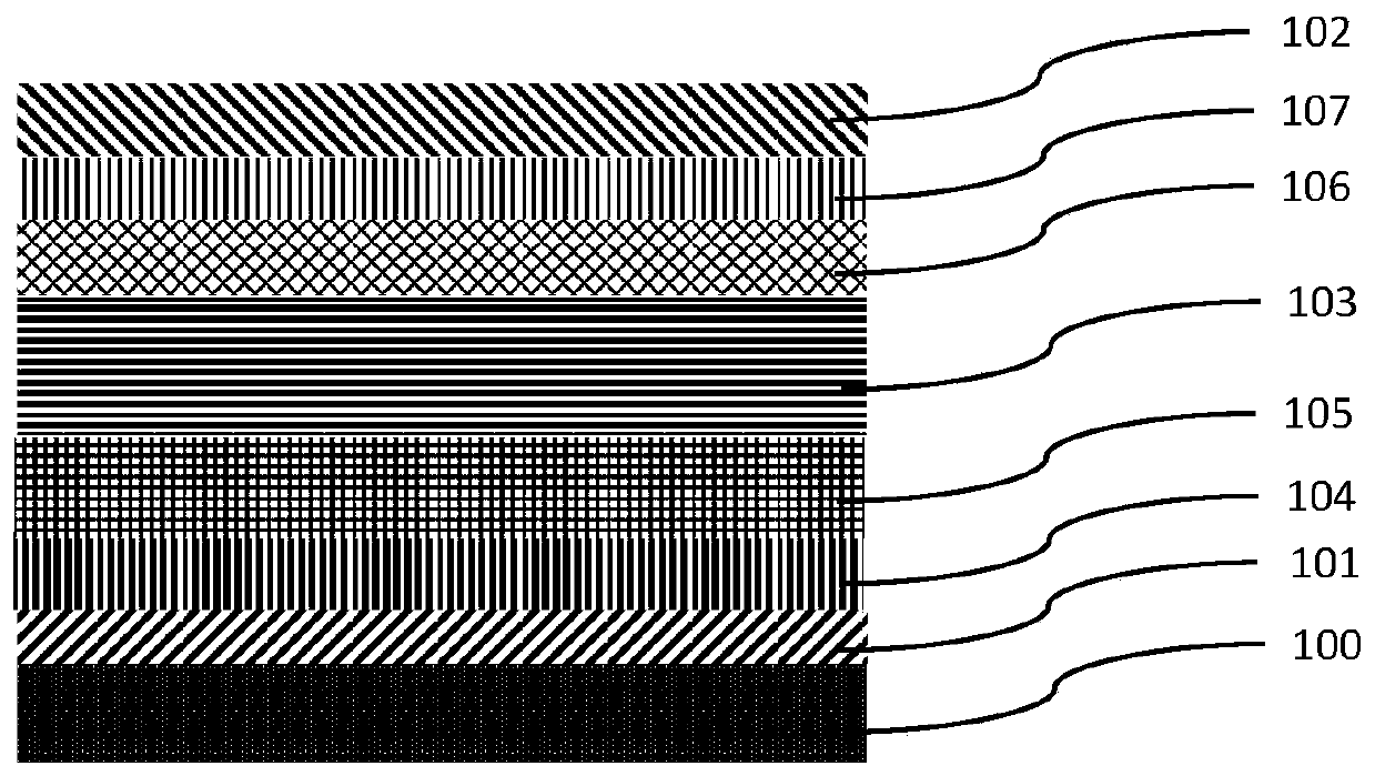
[0061] The present embodiment is an electroluminescence device, the structure is:

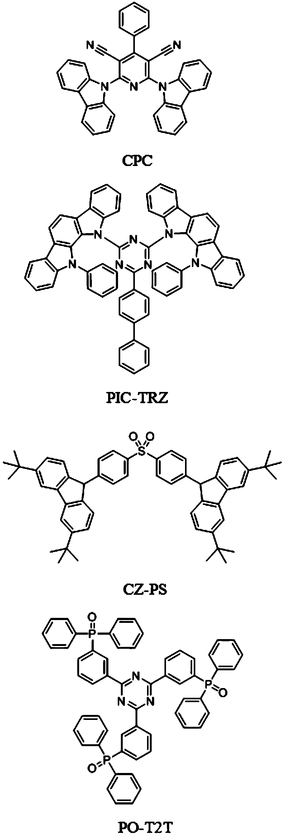
[0062] ITO / PEDOT:PSS / TFB / DCzIPN:(CdSe / ZnS quantum dot) / PO-T2T / LiF / Al.

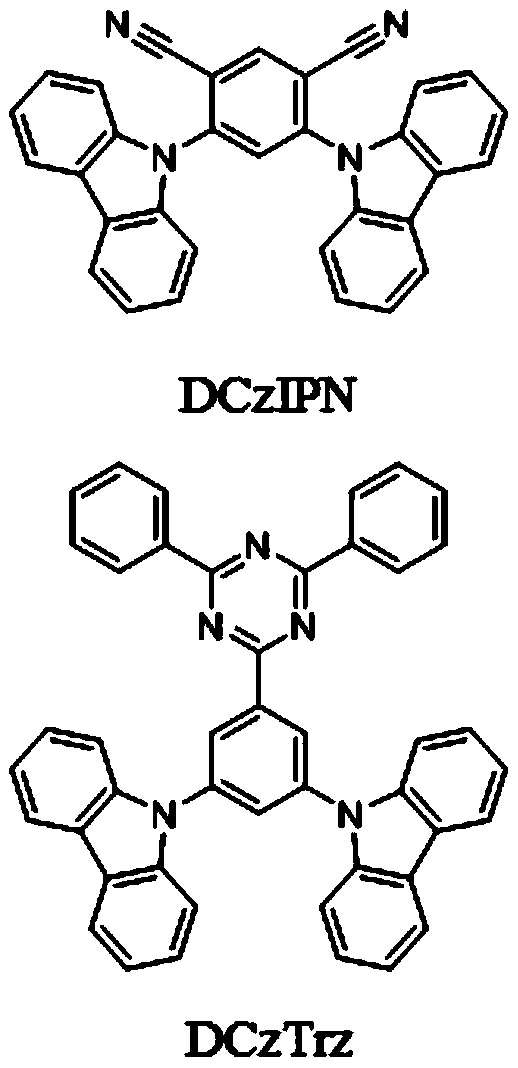
[0063] Among them, the light-emitting layer uses the organic material DCzIPN as the energy donor material, the decay lifetime of the excited state is 1.2 microseconds, the peak wavelength of the emission spectrum is 447nm, and the energy level difference between the singlet state and the triplet state is 0.05eV;

[0064] CdSe / ZnS quantum dots (CdSe / ZnS quantum dots) are used as nanocrystalline semiconductor materials, the decay lifetime of the excited state is 0.05 microseconds, and the peak wavelength of the emission spectrum is 626nm.

[0065] The preparation steps of the above-mentioned electroluminescent device are as follows:

[0066] (1) Substrate treatment: Clean the surface of the substrate with glass cleaner and pure water successively, dry it with nitrogen, bake at 150°C for 1 hour, and treat it with UV for 5 min...

Embodiment 2

[0072] The present embodiment is an electroluminescence device, the structure is:

[0073] ITO / PEDOT:PSS / TFB / DCzTrz:(InP / ZnSeS quantum dot) / PO-T2T / LiF / Al.

[0074] Among them, the light-emitting layer uses the organic material DCzTrz as the energy donor material, the decay lifetime of the excited state is 3.1 microseconds, the peak wavelength of the emission spectrum is 440nm, and the energy level difference between the singlet state and the triplet state is 0.25eV;

[0075] Taking InP / ZnSeS quantum dot (InP / ZnSeS quantum dot) as the nano-crystal semiconductor material, the decay lifetime of the excited state is 0.03 microseconds, and the emission spectrum peak wavelength is 520nm.

[0076] The above electroluminescent device was prepared similarly to Example 1.

Embodiment 3

[0078] The present embodiment is an electroluminescence device, the structure is:

[0079] ITO / PEDOT:PSS / TFB / CPC:(CdSe / ZnS quantum dot) / PO-T2T / LiF / Al.

[0080] Among them, the light-emitting layer uses the organic material CPC as the energy donor material, the decay lifetime of the excited state is 47 microseconds, the peak wavelength of the emission spectrum is 490nm, and the energy level difference between the singlet state and the triplet state is 0.04eV;

[0081] Taking (CdSe / ZnS quantum dot) as a nanocrystalline semiconductor material, the decay lifetime of its excited state is 0.05 microseconds, and the peak wavelength of the emission spectrum is 626nm.

[0082] The above electroluminescent device was prepared similarly to Example 1.


PUM


Abstract

The invention relates to an electroluminescence device, its light-emitting layer and application. The light emitting layer comprises at least one nanocrystalline semiconductor material, and at least one organic light emitting material; the emission spectrum of the organic light emitting material overlaps at least partially the excitation spectrum of the nanocrystalline semiconductor material; the excited state of the organic light emitting material The decay lifetime is greater than 1 microsecond. The present invention innovatively uses an organic luminescent material with a long excited state lifetime, specifically an excited state decay lifetime exceeding 1 microsecond, as the host material, so that the energy of the organic luminescent material can be effectively transferred to the nanocrystal semiconductor material to obtain a High-performance QLED devices can greatly improve the efficiency of electroluminescent devices that use nanocrystalline semiconductor materials as luminescent active components.

Description

technical field [0001] The invention relates to the technical field of light-emitting devices, in particular to an electroluminescence device, a light-emitting layer and applications thereof. Background technique [0002] Nanocrystalline semiconductor materials, also known as nanocrystals, are composed of a limited number of atoms, and at least two dimensions are on the order of nanometers. The two-dimensional space is restricted, and the quantum confinement effect is particularly significant. When excited by light or electricity, nanocrystalline semiconductor materials will emit a spectrum with a very narrow half-peak width (usually less than 40nm), and the luminous color is mainly determined by the particle size. Stability and other characteristics. [0003] Due to the advantages of high luminous efficiency, controllable luminous color, and high color purity, nanocrystalline semiconductor materials have great application potential in next-generation display technologies....

Claims


Application Information

Patent Timeline
Patent Type & Authority Patents(China)
IPC IPC(8): H01L51/50H01L51/54H01L51/56
CPCH10K85/625H10K50/115H10K2102/00H10K71/00
Inventor 李哲谢相伟宋晶尧付东
Owner GUANGDONG JUHUA PRINTING DISPLAY TECH CO LTD
Why Eureka
Try Eureka