
Eureka
For R&D, Eureka makes reading and utilizing patents & technical documents easy.
Eureka AIR
Designed for self-driven R&D workflows. Generate viable solutions, solve complex R&D challenges, empower your innovation with AI.

Eureka Materials
Designed for material experts only. Revolutionize your material R&D, from search, analyze, to developing new materials.

TechResearch
Generate reliable direction feasibility study reports for your R&D in just a few steps.

TechSeek
Discover and master advanced knowledge NOW. Basics, ideas, possibilities, all at once.

TechMind
As an expert in R&D Theories, TechMind can generates customized viable solutions instantly.

TechRisk
Analyze your overall solution with one click, know your potential R&D risks in advance.

TechMonitor
Get weekly tech updates, stay abreast of the latest tech innovations and key insights.
Semiconductor wafer processing method
A processing method and semiconductor technology, which is applied in semiconductor/solid-state device manufacturing, metal processing equipment, manufacturing tools, etc., to achieve the effect of alleviating curing shrinkage, reducing surface ripples, and alleviating the impact of fluidity
- Summary
- Abstract
- Description
- Claims
- Application Information
AI Technical Summary
Problems solved by technology
Method used
Image

Examples
Embodiment 1
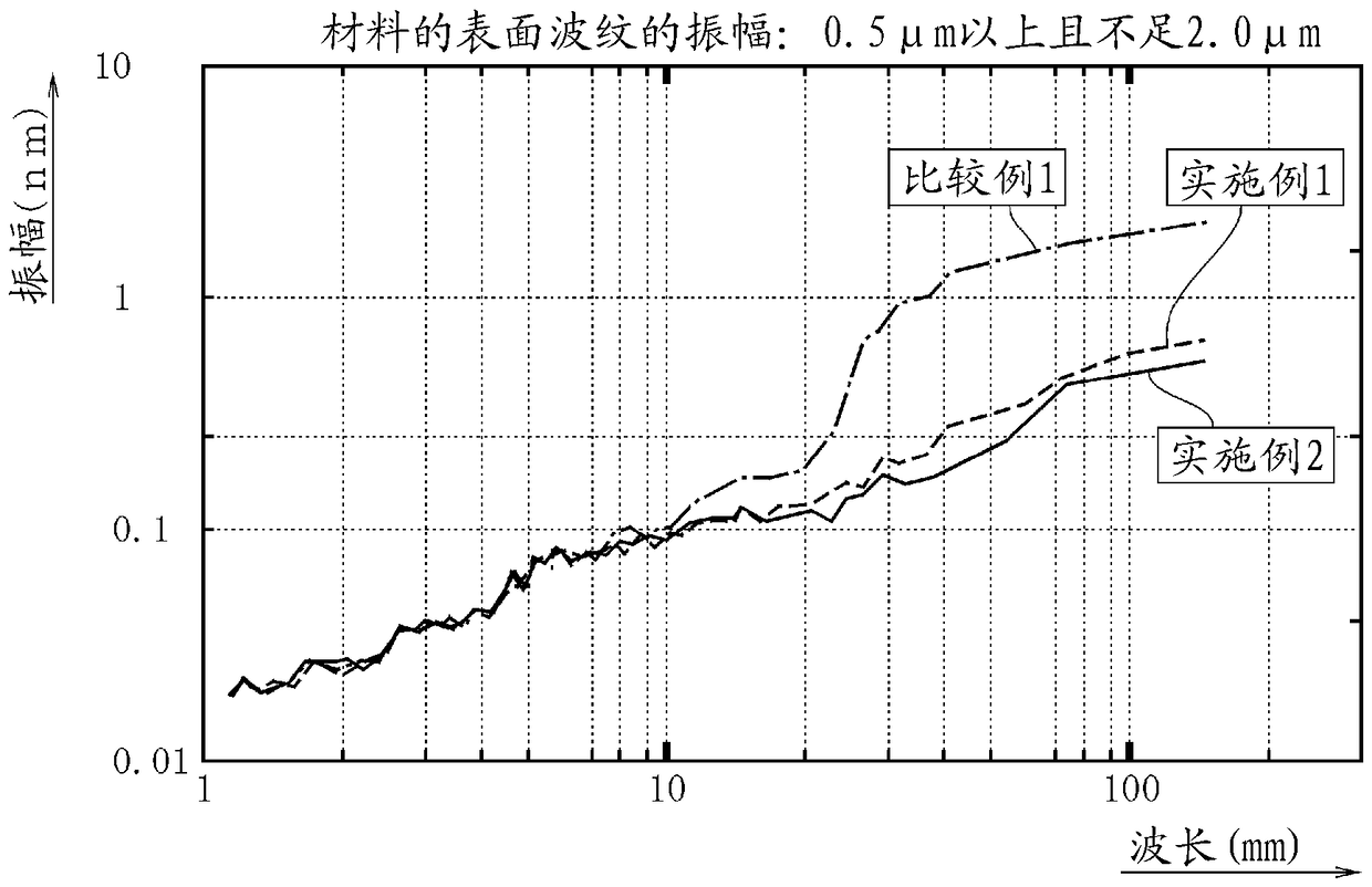
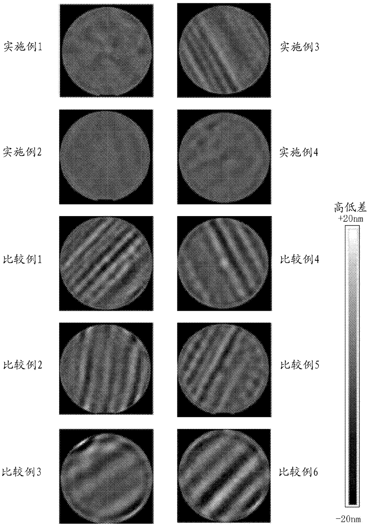
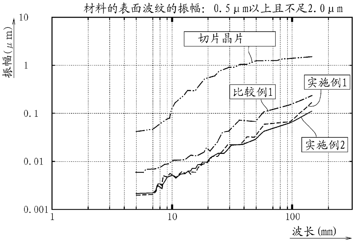
[0050] First, a silicon single crystal ingot is cut (sliced) by a multi-wire saw device using a fixed abrasive grain system to produce a plurality of silicon wafers with a diameter of 300 mm. Then, frequency analysis is performed on the surface height of the first surface 11 of the wafer 10, and the amplitude of the surface waviness 11a (the amplitude of the surface waviness of the material) of the first surface 11 of the wafer 10 in the wavelength range of 10 to 100 mm is selected to be 0.5 μm or more. and less than 2.0 μm wafer 10 ( Figure 4 (a)). After the first surface 11 of the selected wafer 10 is coated with a UV curable resin as a curable material through the first coating layer forming process ( Figure 4 (b)) The curable material made of the UV curable resin is cured in the first coating layer curing step to form the first coating layer 21 on the first surface 11 of the wafer 10 . Next, on the surface of the first coating layer 21 formed on the first surface 11 of...
Embodiment 2
[0052] A double-sided polished wafer was obtained in the same manner as in Example 1 except that the coating layer forming step and the coating layer curing step were repeated three times. This wafer was referred to as Example 2.
Embodiment 3
[0054] Carry out frequency analysis on the surface height of the first surface of the wafer, except that the amplitude of the surface waviness on the first surface of the wafer (the amplitude of the surface waviness of the material) in the wavelength region of 10 to 100 mm is selected to be 2.0 μm or more, and the implementation In Example 1, a double-sided polished wafer was obtained in the same manner. This wafer was referred to as Example 3.
PUM
 Abstract
Description
Claims
Application Information
 - R&D Engineer
- R&D Manager
- IP Professional
- Industry Leading Data Capabilities
- Powerful AI technology
- Patent DNA Extraction
Browse by: Latest US Patents, China's latest patents, Technical Efficacy Thesaurus, Application Domain, Technology Topic, Popular Technical Reports.
© 2024 PatSnap. All rights reserved.Legal|Privacy policy|Modern Slavery Act Transparency Statement|Sitemap|About US| Contact US: help@patsnap.com