Preparation method of two-color single photon source structure, and prepared structure
A single-photon source, two-color technology, applied in the structure of the active region, nano-optics, nano-technology, etc., to achieve the effects of good controllability, adjustable wavelength, and simple preparation process
- Summary
- Abstract
- Description
- Claims
- Application Information
AI Technical Summary
Problems solved by technology
Method used
Image
Examples
Embodiment 1
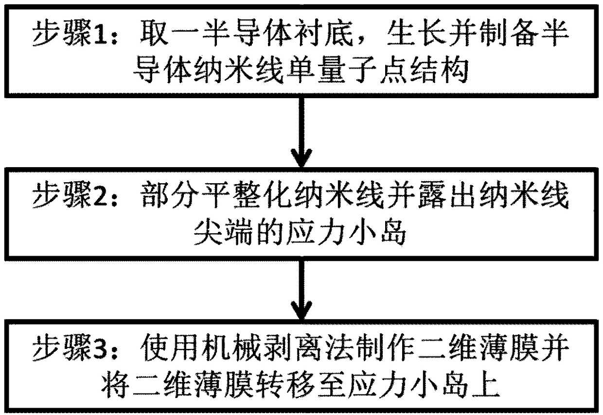
[0028] This embodiment provides a method for preparing a two-color single-photon source structure, figure 1 For the preparation flow diagram of the preparation method, combined with figure 2 , the preparation method provided by the invention comprises the following steps:
[0029] The first step is to grow and prepare the nanowire single quantum dot structure 2 on the semiconductor substrate 1 .
[0030] In this embodiment, the nanowire single quantum dot structure 2 can be prepared by way 1) or way 2):
[0031] 1) GaN / AlN or InAs / InP nanowire single quantum dot structure 2 grown by droplet autocatalysis; the quantum dot is located in the axial direction of the nanowire, and the substrate 1 is non-selective;
[0032] 2) Growth of InAs / GaAs, GaAs / AlGaAs or InAs / InP self-organized quantum dots, the density of self-organized quantum dots is less than 10 -8 / cm -2 , and then use the quantum dot fluorescence imaging method, and use electron beam exposure combined with inductiv...
Embodiment 2
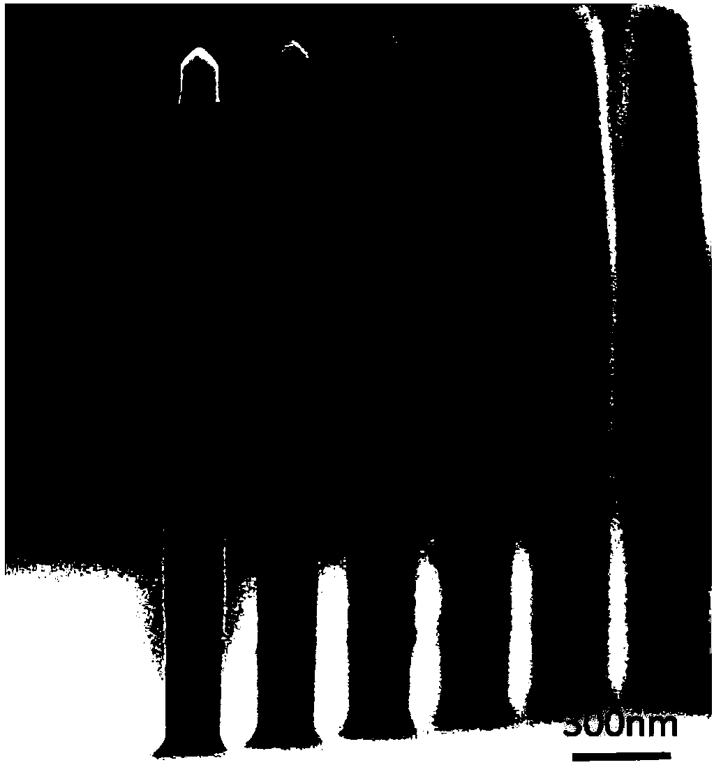
[0040] This embodiment provides a two-color single-photon source structure, the process of its preparation is as follows figure 1 As shown, the prepared structure is as figure 2 , 3 shown.
[0041] Its preparation process is as follows:
[0042] S1. growing and preparing a nanowire single quantum dot structure 2 on a semiconductor substrate 1;
[0043] S2. Partially planarize the nanowire single quantum dot structure 2 to expose the stress island 3 at the top of the nanowire;
[0044] S3. Fabricate the two-dimensional film 4 by using a mechanical lift-off method, and transfer the two-dimensional film 4 to the stress island 3 to complete the preparation.
[0045] In the above scheme, the two-color single-photon source structure provided by the present invention can use the stress island 3 at the top of the nanowire to make the two-dimensional film 4 produce defect-emitting or localized high-brightness excitonic states 5, and then combine with its own single quantum dot Th...
PUM
| Property | Measurement | Unit |
|---|---|---|
| Height | aaaaa | aaaaa |
| Height | aaaaa | aaaaa |
Abstract
Description
Claims
Application Information


