Polishing device and method utilizing in-situ sputtering combined with ion beam etching

An ion beam etching and polishing device technology, applied in the field of ion beams, can solve the problems of not integrating the ion beam sputtering deposition function, reducing the ion beam processing efficiency, etc., so as to overcome the edge effect, improve the speed of vacuuming and the speed of inflation , the effect of reducing process time

Active Publication Date: 2018-08-10
XIAN TECH UNIV
View PDF7 Cites 11 Cited by
  • Summary
  • Abstract
  • Description
  • Claims
  • Application Information

AI Technical Summary

Problems solved by technology

At the same time, the National University of Defense Technology developed a dual vacuum chamber ion beam polishing system (see patent CN 102744654 A) on its original basis. Although an auxiliary vacuum chamber was added to the original equipment, the The auxiliary vacuum chamber completes the workpiece loading, and after the workpiece is completely separated from the self-positioning device in the vacuum chamber, the workpiece transfer device must return to the auxiliary vacuum chamber, which reduces the efficiency of ion beam processing, and this equipment can only be used for etching and polishing without integrated Ion beam sputtering deposition function, in terms of ion source, adopts small-diameter ion source combined with scanning motion to process workpiece

Method used


Image

  • Polishing device and method utilizing in-situ sputtering combined with ion beam etching
  • Polishing device and method utilizing in-situ sputtering combined with ion beam etching
  • Polishing device and method utilizing in-situ sputtering combined with ion beam etching

Examples


Embodiment Construction

[0045] In order to make the object, technical solution and advantages of the present invention clearer, the present invention will be further described in detail below in conjunction with the accompanying drawings and embodiments. It should be understood that the specific embodiments described here are only used to explain the present invention, not to limit the present invention.

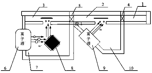
[0046] This embodiment provides a polishing device using in-situ sputtering combined with ion beam etching (see figure 1 ), including a transfer chamber 1 and a sputtering deposition chamber, characterized in that it also includes an etching chamber, and a first slide valve 4 for controlling its communication and closing is arranged between one end of the transfer chamber 1 and the etching chamber, so A second slide valve 5 is set between the etching chamber and the sputtering deposition chamber to control its connection and closure. The other end of the transfer chamber 1 is the outlet of the tran...


PUM


Abstract

The invention relates to the technical field of ion beams, in particular to a polishing device and method utilizing in-situ sputtering combined with ion beam etching. The polishing device comprises atransfer chamber, an etching chamber, a sputtering deposition chamber and gate valves, the gate valves are arranged between the transfer chamber and the etching chamber as well as between the etchingchamber and the sputtering deposition chamber, and workpiece conveying devices for conveying workpieces among the transfer chamber, the etching chamber and the sputtering deposition chamber are arranged in the transfer chamber, the etching chamber and the sputtering deposition chamber. The polishing method applying the polishing device comprises the processes that the workpieces are loaded in thetransfer chamber first, then the workpieces are subjected to ion beam cleaning in the etching chamber, then a layer of thin film layer (sacrificial layer) is deposited on each workpiece in a sputtering mode in the sputtering deposition chamber, then the workpieces are subjected to ion beam correction polishing in the etching chamber, finally, the workpieces are taken out through the transfer chamber, and polishing of optical elements is achieved.

Description

technical field [0001] The invention relates to the technical field of ion beams, in particular to a polishing device and a polishing method utilizing in-situ sputtering combined with ion beam etching. Background technique [0002] Ion beam sputtering deposition can be traced back to the 1970s when it was used to prepare interference optical films, but the quality of the films prepared by this technology was not high until the emergence of wide-beam ion sources, so that ion beam sputtering technology A major breakthrough occurred and optical films with good mechanical properties, strong adhesion and low surface roughness were successfully prepared. At present, with the rapid development of science and technology, this technology has become more mature and perfect abroad, and its application fields are constantly being broadened. However, in China, although the research on ion beam sputtering technology has gradually increased in recent decades, there is still a gap compared...

Claims


Application Information

Patent Timeline
Patent Type & Authority Applications(China)
IPC IPC(8): C23F4/00C23C14/46
CPCC23C14/46C23F4/00
Inventor 刘卫国周顺葛少博王泉惠迎雪蔡长龙陈智利秦文罡刘欢
Owner XIAN TECH UNIV
Why Eureka
Try Eureka