Special ink for assistance in manufacture of backdrill and PCB (printed circuit board) backdrilling method

A back-drilling and ink technology, which is applied in ink, applications, household appliances, etc., can solve problems such as plug holes, the inability to accurately control the back-drilling depth to the target layer 105 distance, and the inability to realize the control of copper retention in back-drilling, etc., to achieve The effect of production process optimization and precise copper retention height control

Active Publication Date: 2018-08-17
DONGGUAN SHENGYI ELECTRONICS
View PDF7 Cites 4 Cited by
  • Summary
  • Abstract
  • Description
  • Claims
  • Application Information

AI Technical Summary

Problems solved by technology

[0002] At present, the precision control of back-drilling STUB in the industry is still a common technical problem. STUB means that after the circuit board is drilled and plated, the plated hole is drilled through back-drilling (the diameter of the drill hole is larger than that of the plated hole), and the plated hole is drilled to a certain depth. Finally, the length of the remaining copper from the bottom of the back-drilled hole wall to the non-drilled layer is the STUB. At present, the STUB accuracy control mainly depends on the accuracy improvement of the drilling equipment and the uniformity control of the plate thickness. The current back-drilling technology is actually The depth-controlled drilling technology adopts the construction of the zero height of the drilling hole, and then sets a certain drilling depth value to complete the back-drilling. When the plate thickness fluctuates, it is impossible to achieve accurate back-drilling copper retention control. In addition, when back-drilling, At present, the problem of back-drilling copper wire/copper broken plug holes with high thickness-to-diameter ratio is a problem that

Method used


Image

  • Special ink for assistance in manufacture of backdrill and PCB (printed circuit board) backdrilling method
  • Special ink for assistance in manufacture of backdrill and PCB (printed circuit board) backdrilling method
  • Special ink for assistance in manufacture of backdrill and PCB (printed circuit board) backdrilling method

Examples


Embodiment Construction

[0019] In order to explain in detail the technical solutions adopted by the present invention to achieve the intended technical purpose, the technical solutions in the embodiments of the present invention will be clearly and completely described below in conjunction with the accompanying drawings in the embodiments of the present invention. Obviously, the described implementation Examples are only part of the embodiments of the present invention, rather than all embodiments, and, on the premise of not paying creative work, the technical means or technical features in the embodiments of the present invention can be replaced, the following will refer to the accompanying drawings and combine Examples illustrate the present invention in detail.

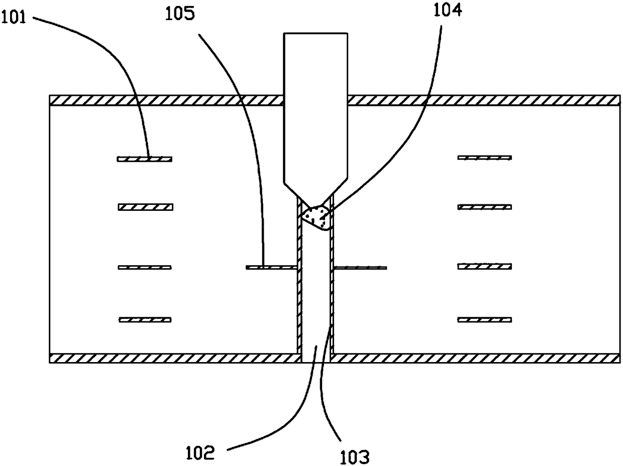
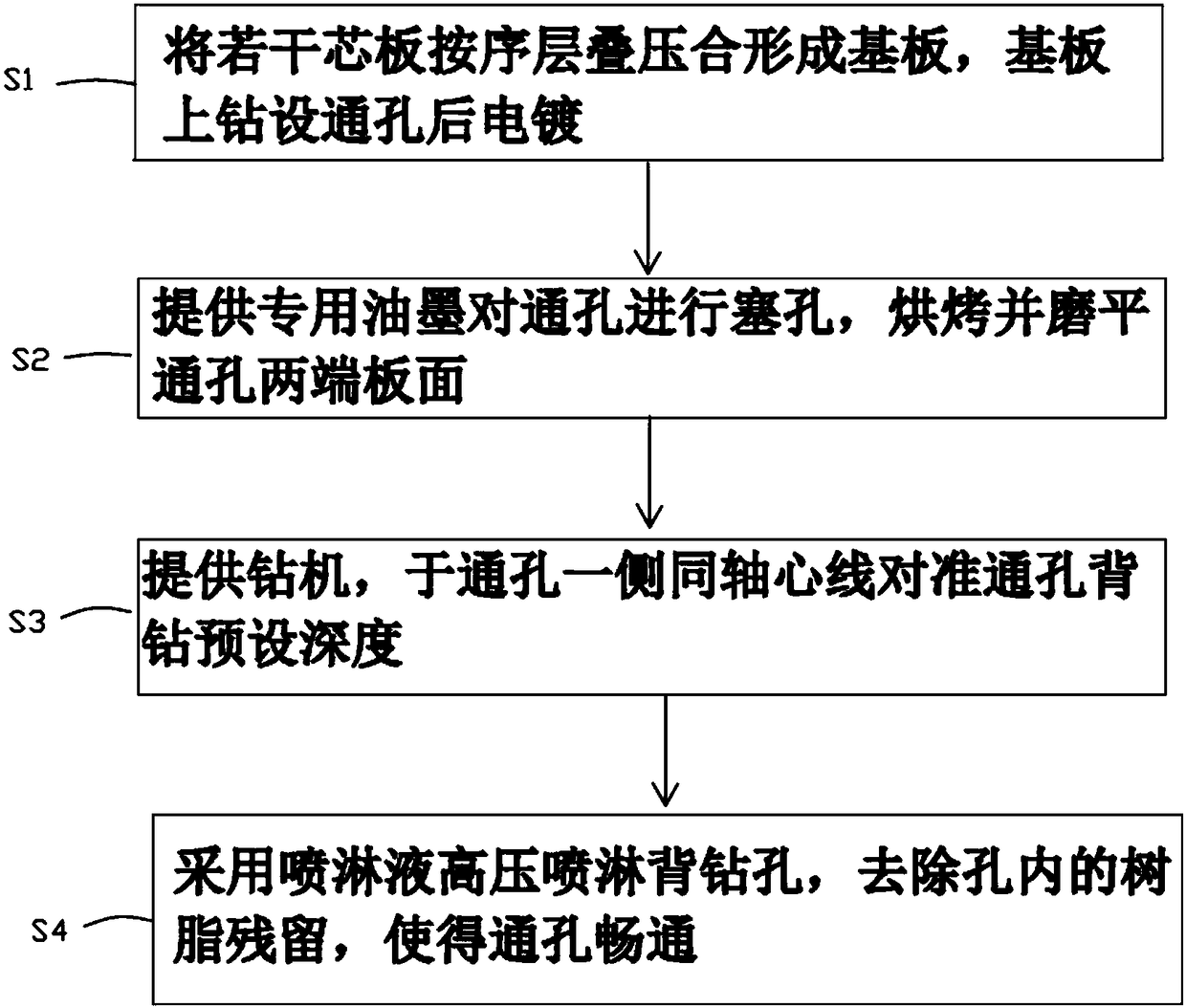
[0020] figure 2 As shown, the present invention provides a method for drilling holes on a PCB, which is realized by a brand-new process route, including the following steps: 1) stacking and laminating several core boards in order to form...


PUM


Abstract

The invention provides special ink for assistance in the manufacture of a backdrill and a PCB (printed circuit board) backdrilling method. The special ink is mainly made from propylene glycol monomethyl acetate, pumice powder and water-soluble resin, wherein the propylene glycol monomethyl acetate accounts for 20-25% by mass, the pumice powder accounts for 50-60% by mass, and the water-soluble resin accounts for 20-25% by mass. The PCB backdrilling method comprises the steps of 1) stacking a plurality of core plates in order to form a substrate, drilling the substrate to obtain via holes, andplating; 2) providing the special ink to plug the via holes, baking, and grinding the end faces of the via holes; 3) drilling a drill rig, and backdrilling to a preset depth on one side of the via holes, with coaxial alignment to the via holes; 4) subjecting the backdrilled holes to high pressure spraying via a spraying liquid so as to remove resin residue in the holes, so that the via holes are smooth. The problem that large-thickness and -diameter copper wires/fragments block the via holes is successfully solved.

Description

technical field [0001] The invention relates to a back-drilling method on a printed circuit board (PCB). Background technique [0002] At present, the precision control of back-drilling STUB in the industry is still a common technical problem. STUB means that after the circuit board is drilled and plated, the plated hole is drilled through back-drilling (the diameter of the drill hole is larger than that of the plated hole), and the plated hole is drilled to a certain depth. Finally, the length of the remaining copper from the bottom of the back-drilled hole wall to the non-drilled layer is the STUB. At present, the STUB accuracy control mainly depends on the accuracy improvement of the drilling equipment and the uniformity control of the plate thickness. The current back-drilling technology is actually The depth-controlled drilling technology adopts the construction of the zero height of the drilling hole, and then sets a certain drilling depth value to complete the back-dr...

Claims


Application Information

Patent Timeline
IPC IPC(8): C09D11/107C09D11/03B26F1/16
CPCB26F1/16B26F2210/08C09D11/03C09D11/107
Inventor 何平刘梦茹文贵宜朱多丰
Owner DONGGUAN SHENGYI ELECTRONICS
Why Eureka
Try Eureka