Semi-bent printed circuit board and manufacturing method thereof

A technology for printed circuit boards and manufacturing methods, which is applied in the fields of printed circuit manufacturing, printed circuits, printed circuit components, etc., can solve the problems of high cost, long cycle, and complicated processing process of rigid-flexible boards, and achieve the goal of processing methods Simple, reliable, and solve the effect of solder resist cracking

Active Publication Date: 2020-07-10
KALEX MULTI LAYER CIRCUIT BOARD (ZHONGSHAN) CO LTD
View PDF9 Cites 0 Cited by
  • Summary
  • Abstract
  • Description
  • Claims
  • Application Information

AI Technical Summary

Problems solved by technology

PI film has excellent flexural performance but high cost, which leads to high price of its derivative PCB products, but in some occasions with low flexural requirements or static flexure, such high flexural properties are not required; and , the processing flow of the rigid-flex board is complicated and the cycle is long

Method used


Image

  • Semi-bent printed circuit board and manufacturing method thereof
  • Semi-bent printed circuit board and manufacturing method thereof
  • Semi-bent printed circuit board and manufacturing method thereof

Examples


Embodiment 1

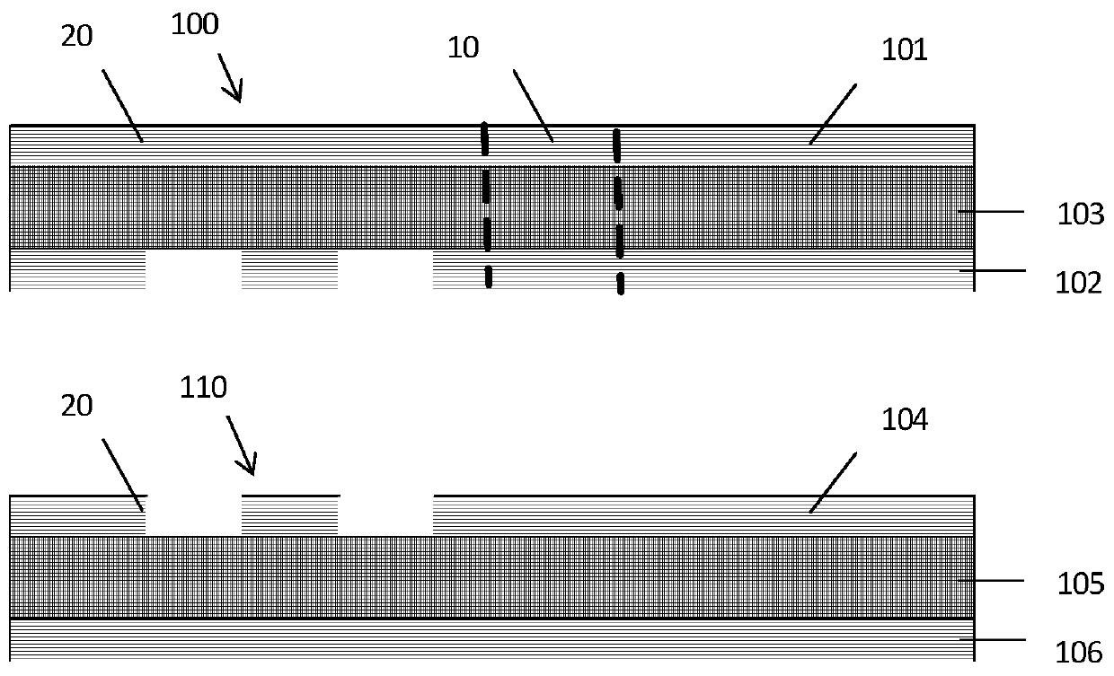
[0037] This embodiment provides a half-bent printed circuit board and a manufacturing method thereof. The preparation method comprises the following steps:

[0038] Step (1), see figure 1 : take the first double-sided copper-clad laminate and make the inner layer circuit to form the first inner layer circuit board 100 including the first outer layer copper foil layer 101 and the first inner layer circuit layer 102; the first inner layer circuit board 100 It is divided into a non-bending area 20 and a bending area 10; the copper-free area of ​​the first inner circuit layer 102 in the bending area 10 is provided with a non-conducting line, and at least one end of the non-conducting line extends into the non-bending area. area, and the non-conductive line is not in contact with the conductive line of the first inner circuit layer 102 .

[0039] In this embodiment, the first double-sided copper-clad laminate is a common double-sided copper-clad laminate in the field, including t...

Embodiment 2

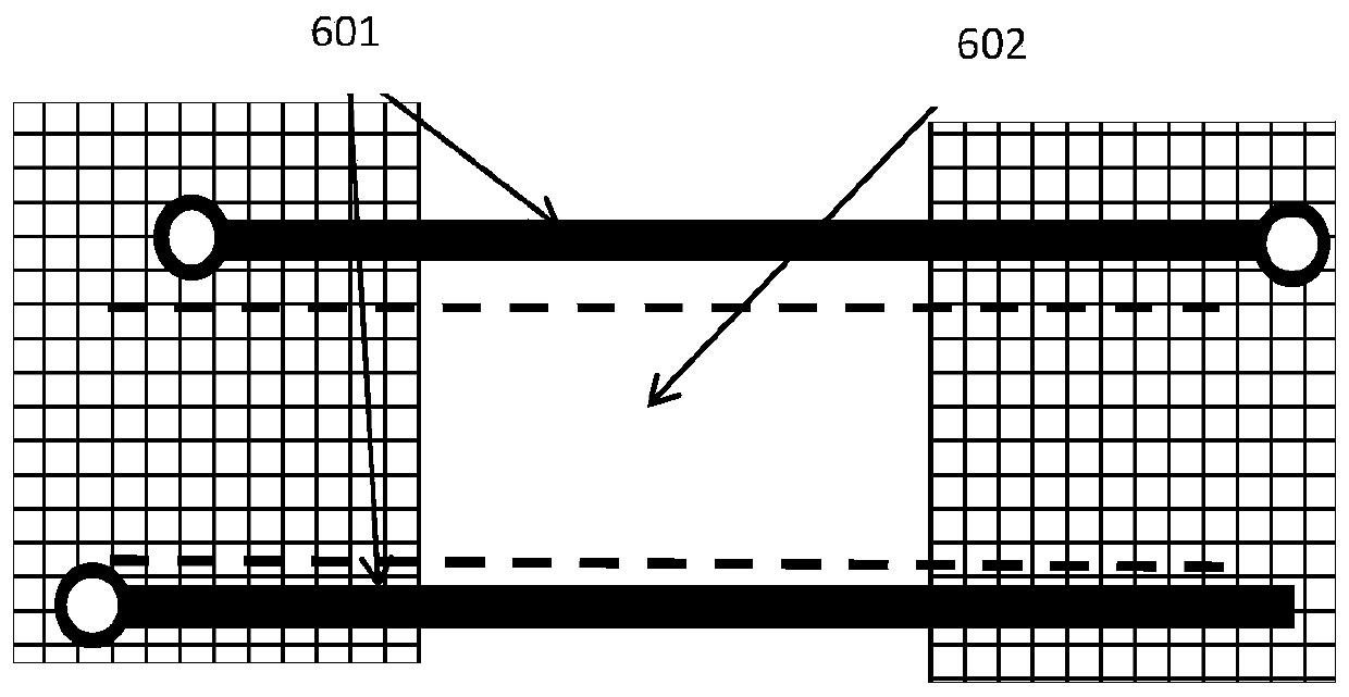
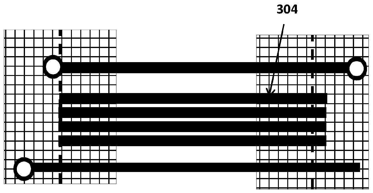
[0065] This embodiment is a modification example of Embodiment 1, and also provides a half-bent printed circuit board and a manufacturing method thereof. Compared with the preparation method of embodiment 1, the changes of this production method mainly include:

[0066] In step (1): the non-conducting line 304 satisfies the following conditions:

[0067] 1) The non-conductive wire is copper wire ( Figure 4 middle a);

[0068] 2) Conductive wire ( Figure 4 Middle b) and the non-conductive line 304 ( Figure 4 Middle a) is consistent with the bending direction;

[0069] 3) The minimum distance e between the preset component hole or pad and the boundary of the bending area in the non-bending area is 1 mm. At the same time, the distance c of the non-conducting line extending out of the bending area is 1mm;

[0070] 4) The width and line gap of the non-conducting line a are equal to 2 mm.

[0071] In step (5), the total thickness of the first ink layer and the second ink l...


PUM


Abstract

The invention provides a half-bent printed circuit board and a making method thereof. The making method includes: pre-arranging a bent area on an inner-layer circuit board; arranging non-conducting wires in a copper-free area of an inner-layer circuit layer of the bent area; especially arranging non-conducting wires in a copper-free area of an outer-layer circuit layer in a matched manner; especially arranging the non-conducting wires according a specific layout mode to form a specific half-bent circuit board making process. The half-bent circuit board made by the making process can reduce stress directly acting on the circuit board in the process of bending, the problem that the inner-layer circuit board in the bent area cracks during board bending is solved, certain bending needs are metwithout adopting expensive PI films, and cost reduction and meeting of bending needs are well balanced; the half-bent circuit board has high reliability and excellent thermostability.

Description

technical field [0001] The invention relates to a circuit board, in particular to a half-bent printed circuit board and a manufacturing method thereof. Background technique [0002] Electronic products are miniaturized and multi-functional, which requires PCB to achieve high density and high performance. Under this premise, bent boards and rigid-flex boards have shown advantages. These boards with special structures can significantly reduce the volume occupied by electronic products and achieve dense assembly and three-dimensional assembly. [0003] At present, the reinforcing material used in the bent copper-clad laminate is PI film, and the reinforcing material used in the bending part of the rigid-flex board is also PI film. PI film has excellent flexural performance but high cost, which leads to high price of its derivative PCB products, but in some occasions with low flexural requirements or static flexure, such high flexural properties are not required; and , The pro...

Claims


Application Information

Patent Timeline
Patent Type & Authority Patents(China)
IPC IPC(8): H05K3/46H05K1/14
CPCH05K1/147H05K3/4691H05K2203/013
Inventor 戴匡
Owner KALEX MULTI LAYER CIRCUIT BOARD (ZHONGSHAN) CO LTD
Why Eureka
Try Eureka